Nanowire-Based Semiconductor Device And Method Employing Removal Of Residual Carriers

a technology of nanowires and semiconductor devices, applied in the direction of semiconductor devices, electrical devices, nanotechnology, etc., can solve the problems of reducing the efficiency of the semiconductor device, reducing the switching speed or modulation rate of the semiconductor nanowire-based device, and reducing the carrier lifetime, so as to facilitate the removal of residual carriers and enhance recombination

Active Publication Date: 2009-07-16
HEWLETT-PACKARD ENTERPRISE DEV LP
View PDF13 Cites 17 Cited by
  • Summary
  • Abstract
  • Description
  • Claims
  • Application Information

AI Technical Summary

Benefits of technology

[0008]In some embodiments of the present invention, a nanowire-based device is provided. The nanowire-based device comprises a semiconductor nanowire having a semiconductor junction. The nanowire-based device further comprises a residual carrier sink. The residual carrier sink is adjacent to a surface of the nanowire proximal to the semiconductor junction. The residual carrier sink facilitates removal of residual carriers from the semiconductor junction using one or both enhanced recombination and direct extraction of residual carriers.

Problems solved by technology

A switching speed or a modulation rate of semiconductor nanowire-based devices may be limited by the presence of residual carriers that remain in or near the semiconductor junction when the device is turned off.
Unfortunately decreasing the carrier lifetime also tends to decrease an efficient of the semiconductor device.

Method used


Image

  • Nanowire-Based Semiconductor Device And Method Employing Removal Of Residual Carriers
  • Nanowire-Based Semiconductor Device And Method Employing Removal Of Residual Carriers
  • Nanowire-Based Semiconductor Device And Method Employing Removal Of Residual Carriers

Examples


Embodiment Construction

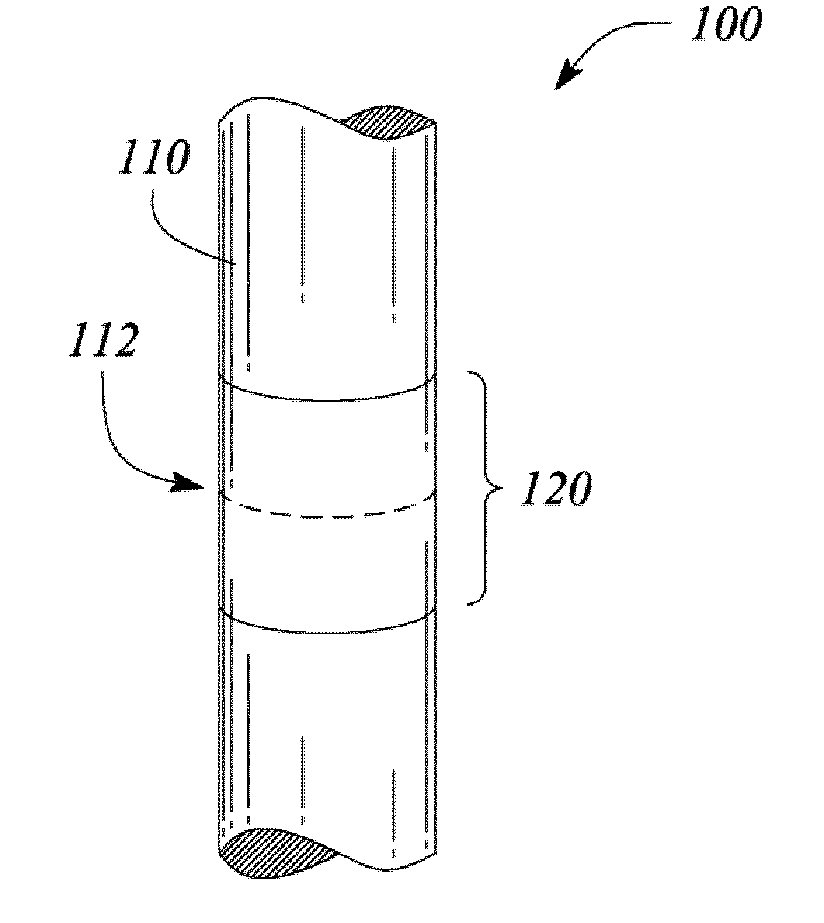
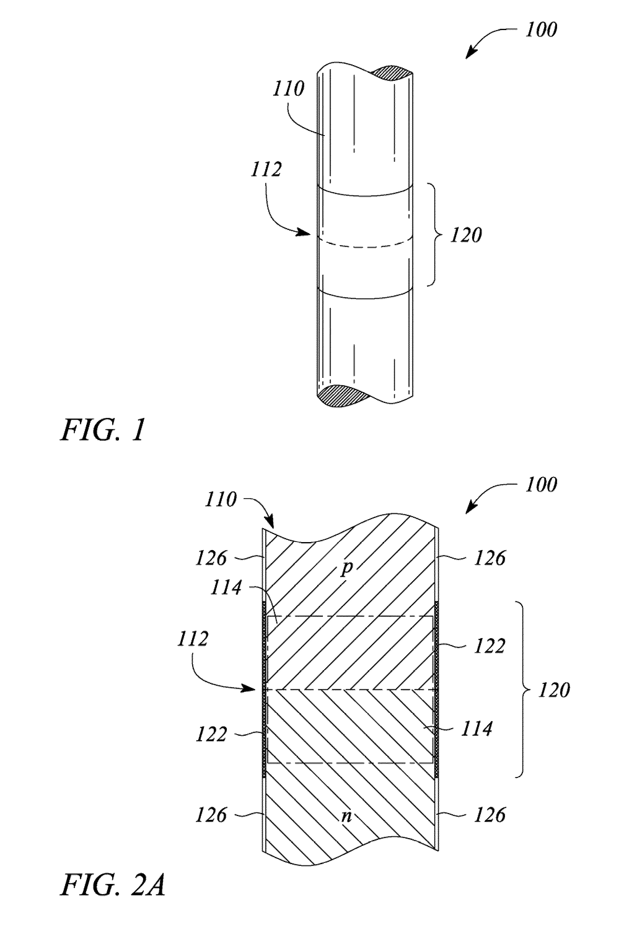
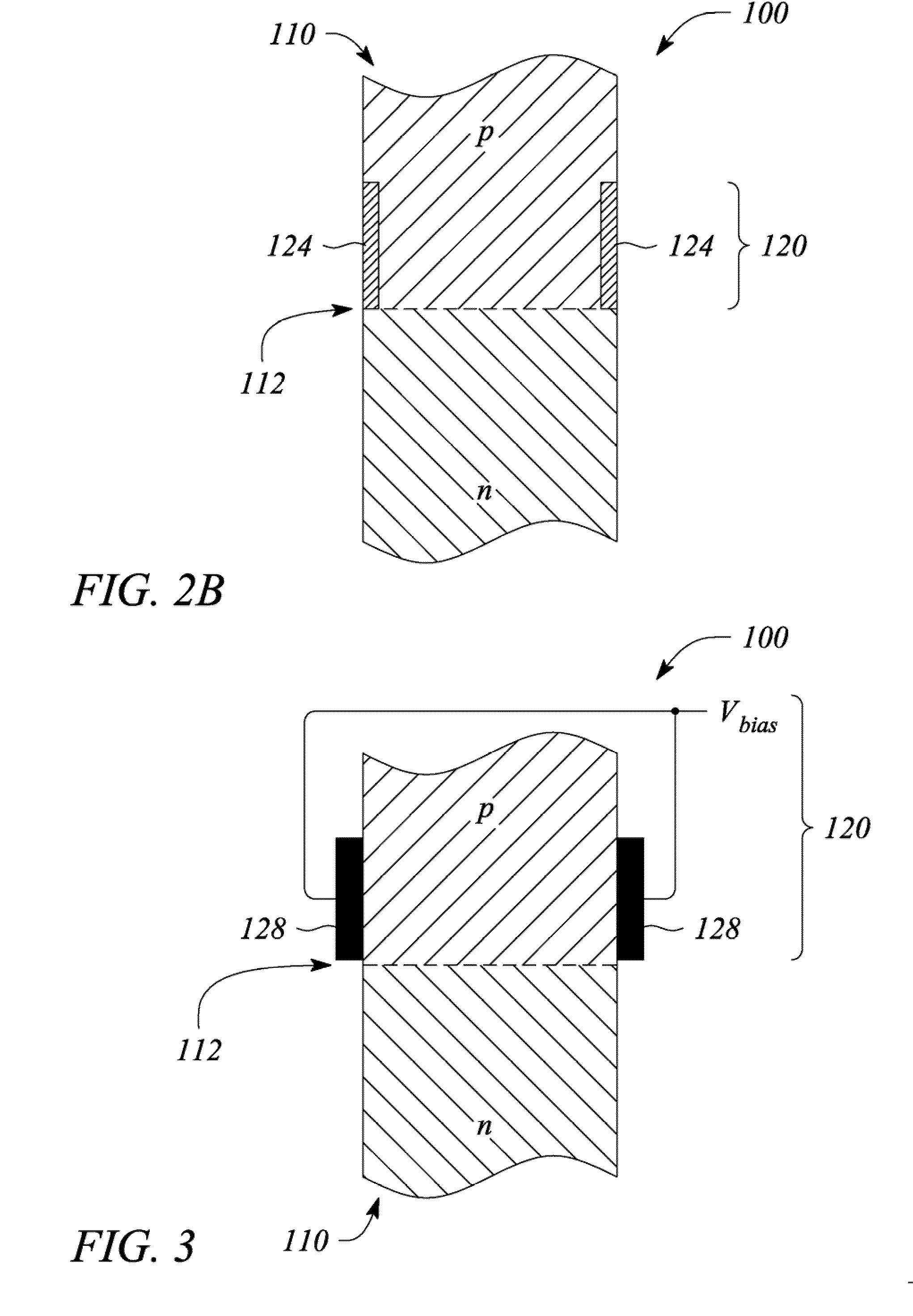
[0019]Embodiments of the present invention facilitate removal of residual carriers from a region of a semiconductor junction of a nanowire-based device. In particular, residual carriers are removed from an active region of the semiconductor junction. According to various embodiments, the residual carrier removal is provided ba residual carrier sink. The present invention applies to residual carrier removal from nanowire-based devices including, but not limited to, photonic devices as well as essentially non-photonic, electronic devices.

[0020]Examples of photonic devices include, but are not limited to light emitting diodes (LEDs), semiconductor lasers, and optical detectors and modulators. Exemplary non-photonic, electronic devices include, but are not limited to, diode junctions used as electronic signal detectors, switches, amplifiers, and modulators. While sometimes described herein with respect to photonic device for simplicity of discussion, unless otherwise specifically noted,...


PUM


Abstract

A nanowire-based device and method employ removal of residual carriers. The nanowire-based device includes a semiconductor nanowire having a semiconductor junction, and a residual carrier sink. The residual carrier sink is located at or adjacent to the semiconductor nanowire near the semiconductor junction and employs one or both of enhanced recombination and direct extraction of the residual carriers. The method includes providing a semiconductor nanowire, forming a semiconductor junction within the semiconductor nanowire, forming a residual carrier sink, and removing residual carriers from the semiconductor junction region using the residual carrier sink.

Description

CROSS-REFERENCE TO RELATED APPLICATION[0001]The present application claims priority from provisional application Ser. No. 61 / 020,469, filed Jan. 11, 2008, the contents of which are incorporated herein by reference in their entirety.STATEMENT REGARDING FEDERALLY SPONSORED RESEARCH OR DEVELOPMENT[0002]N / ABACKGROUND[0003]1. Technical Field[0004]The invention relates to semiconductor devices. In particular, the invention relates to semiconductor devices having a semiconductor junction.[0005]2. Description of Related Art[0006]Semiconductor devices that have need of high switching speeds are being employed in an increasing number of subsytems and systems. Among such high switching speed semiconductor devices are high-frequency electrical components (e.g., microwave and radio frequency switches and amplifying devices), signal emitters (e.g., light emitting diodes or ‘LEDs’, semiconductor lasers, etc.), optical modulators, and signal detectors (e.g., optical detectors, etc.). In recent year...

Claims


Application Information

Patent Timeline
Patent Type & Authority Applications(United States)
IPC IPC(8): H01L29/66H01L21/329
CPCB82Y10/00B82Y20/00H01L29/0665H01L33/18H01L29/0676H01L29/861H01L31/0352H01L29/0673
Inventor KAMINS, THEODORE I.
Owner HEWLETT-PACKARD ENTERPRISE DEV LP
Why Eureka
Try Eureka