
Micromirror device

a micromirror and chip technology, applied in the field of micromirror devices, can solve the problems of unsatisfactory variations in the gap amount between the micromirror chip, the micromirror device may not obtain the desired mirror driving characteristics, and the micromirror device may not obtain the desired heat reliability, etc., to achieve the effect of heat reliability

Inactive Publication Date: 2009-07-30
OLYMPUS CORP
View PDF0 Cites 5 Cited by
  • Summary
  • Abstract
  • Description
  • Claims
  • Application Information

AI Technical Summary

Benefits of technology

[0009]The present invention has been made in consideration of these situations, and an object of the present invention is to provide a micromirror device in which variations in gap amount between the first member and the second member are suppressed, and desired heat reliability is ensured.
[0010]A micromirror device according to the present invention includes a first member, a second member, joining members joining the first member to the second member, and a spacer placed between the first member and the second member. The spacer includes a first surface in surface contact with the first member and a second surface in surface contact with the second member, the first surface being parallel to the second surface. The spacer includes through holes accommodating the joining members, the through holes extending between the first surface and the second surface and including at least one first through hole and second through holes. The joining members includes at least one first joining member accommodated in the first through hole and second joining members accommodated in the second through holes. The first through hole restrains movement of the first joining member in any direction parallel to the first and second surfaces. On the other hand, the second through holes allow movement of the second joining members in at least one direction parallel to the first and second surfaces.
[0011]According to the present invention, there is provided a micromirror device in which variations in gap amount between the first member and the second member are suppressed, and desired heat reliability is ensured.

Problems solved by technology

This may cause a “mirror movement fault” that when the movable mirror portions move about the hinges, the mirror support portion deforms due to lack of rigidity to result in undesirable variations in the gap amount between the micromirror chip and the electrode substrate.
As a consequence, the micromirror device may not obtain desired mirror driving characteristics.
However, with the structure in which the mirror support portion and the electrode substrate are held and restrained by the spacer through a large area, desired heat reliability may not be obtained due to the differences between the linear expansion coefficient of the mirror support portion and electrode substrate and that of the linear expansion coefficient of the spacer.

Method used


Image

  • Micromirror device
  • Micromirror device
  • Micromirror device

Examples


first embodiment

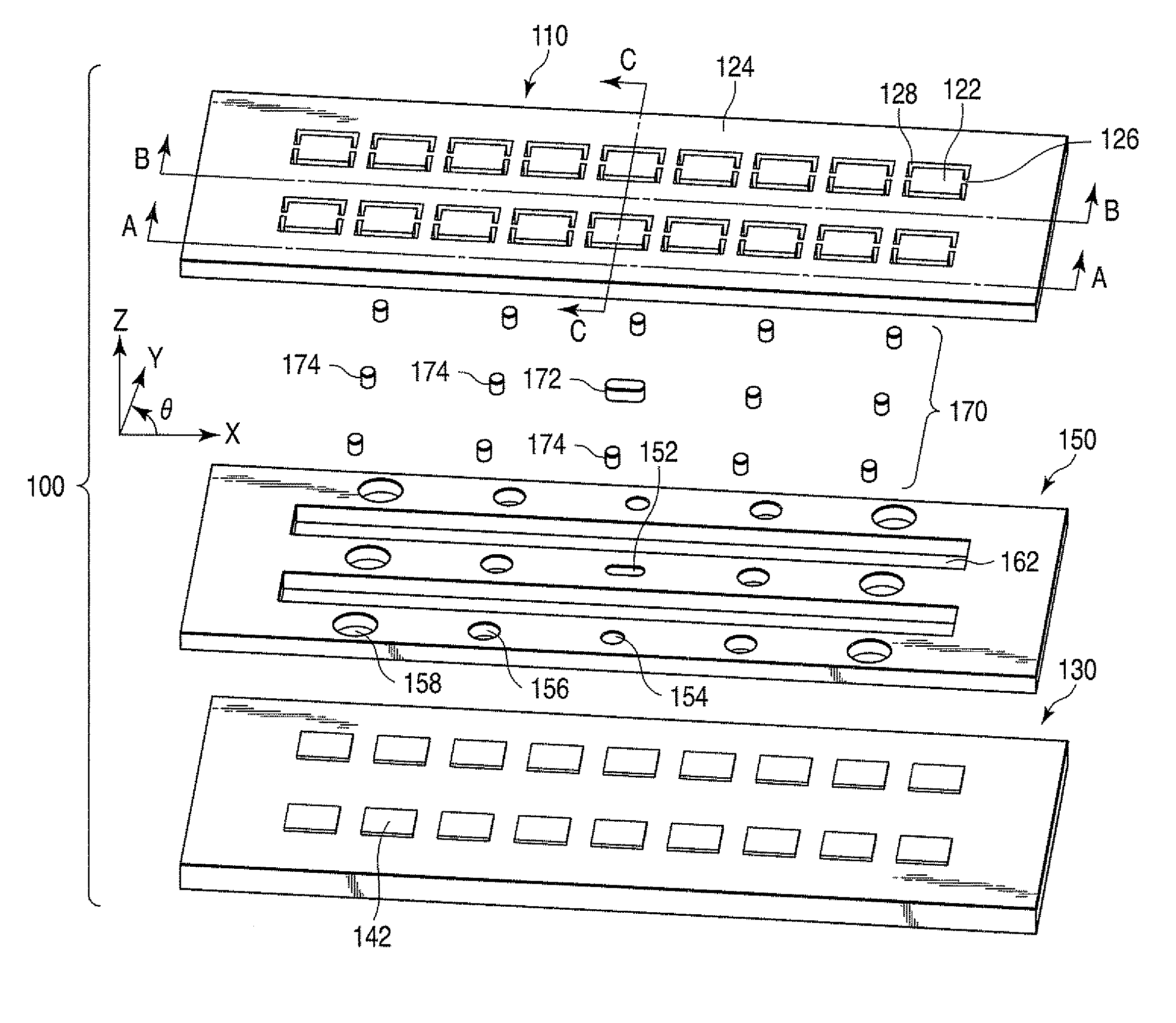
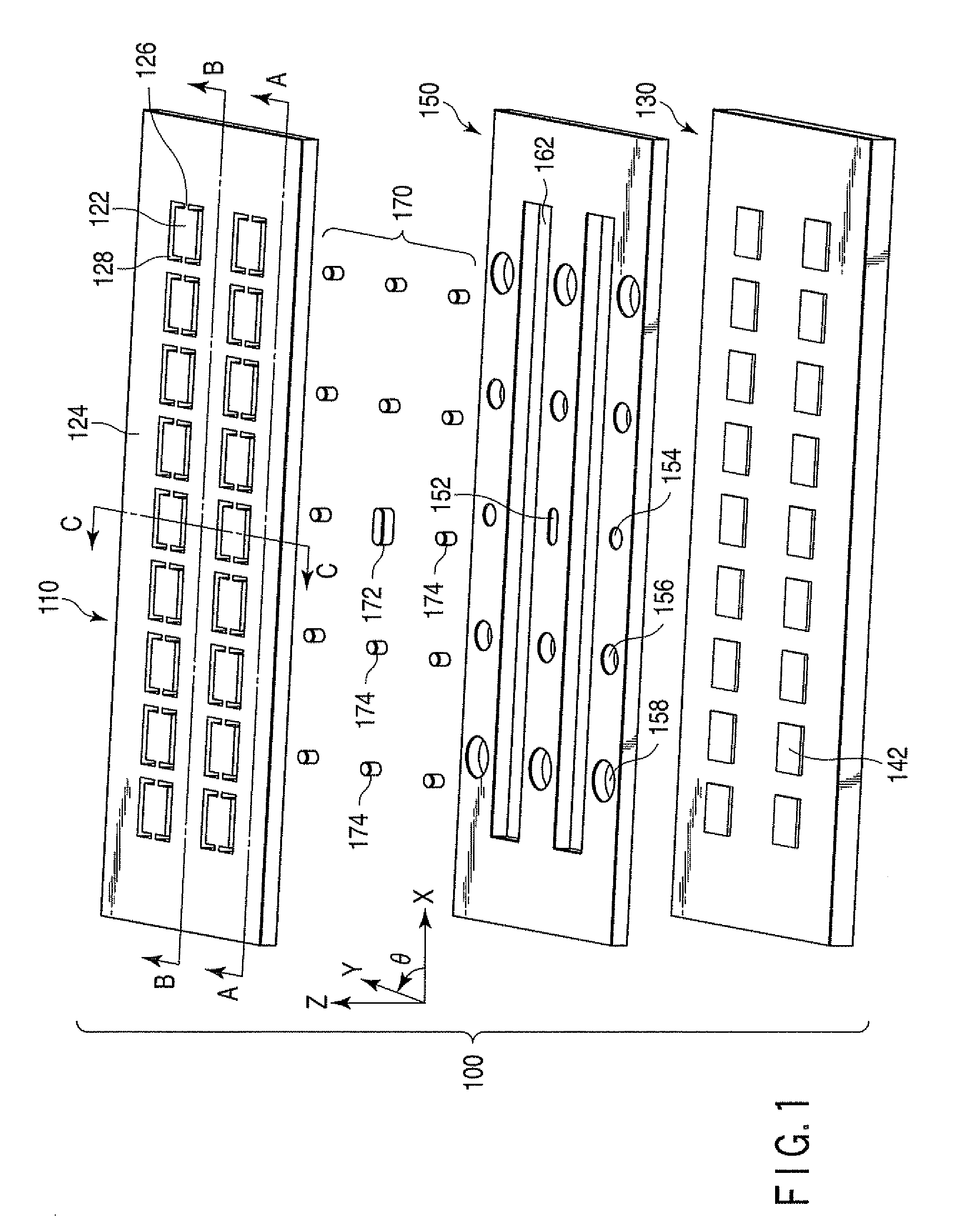
[0023]A micromirror device according to the first embodiment of the present invention will be described with reference to FIGS. 1 to 5. FIG. 1 is an exploded perspective view of the micromirror device according to this embodiment. FIG. 2 is a sectional view taken along a line A-A of the micromirror device shown in FIG. 1. FIG. 3 is a sectional view taken along a line B-B of the micromirror device shown in FIG. 1. FIG. 4 is a sectional view taken along a line C-C of the micromirror device shown in FIG. 1. FIG. 5 is a plan view of a spacer and solder materials shown in FIG. 1. In the following description, an orthogonal coordinate system is set as shown in FIG. 1, and the +Z direction and −Z direction of the orthogonal coordinate system shown in FIG. 1 are respectively the upward and downward directions for the sake of convenience.

[0024]A micromirror device 100 includes a micromirror chip 110 as the first member, an electrode substrate 130 as the second member, a spacer 150 placed bet...

second embodiment

[0054]A micromirror device according to the second embodiment of the present invention will be described with reference to FIGS. 6 to 8. FIG. 6 is an exploded perspective view of the micromirror device according to this embodiment. FIG. 7 is a sectional view taken along a line D-D of the micromirror device shown in FIG. 6. FIG. 8 is a plan view of a spacer and solder materials shown in FIG. 6.

[0055]A micromirror device 200 includes a micromirror chip 210 as the first member, an electrode substrate 230 as the second members a spacer 250 placed between the micromirror chip 210 and the electrode substrate 230, and solder materials 270 as joining members mechanically and electrically joining the micromirror chip 210 to the electrode substrate 230.

[0056]The opposing surfaces of the micromirror chip 210, electrode substrate 230, and spacer 250 are flat. The micromirror chip 210, the electrode substrate 230, and the spacer 250 are in surface contact with each other.

[0057]The spacer 250 has...


PUM


Abstract

A micromirror device includes a first member, a second member, joining members joining the first and second members, and a spacer placed between the first and second members. The spacer includes a first surface in surface contact with the first member, a second surface parallel to the first surface and in surface contact with the second member, at least one first through hole, and second through holes, the first and second through holes extending between the first and second surfaces. The joining members include at least one first joining member accommodated in the first through hole and second joining members accommodated in the second through holes. The first through hole restrains movement of the first joining member in any direction parallel to the first and second surfaces. The second through holes allow movement of the second joining members in at least one direction parallel to the first and second surfaces.

Description

CROSS-REFERENCE TO RELATED APPLICATIONS[0001]This application is based upon and claims the benefit of priority from prior Japanese Patent Application No. 2008-019373, filed Jan. 30, 2008, the entire contents of which are incorporated herein by reference.BACKGROUND OF THE INVENTION[0002]1. Field of the Invention[0003]The present invention relates to a micromirror device.[0004]2. Description of the Related Art[0005]For example, Jpn. Pat. Appln. KOKAI Publication No. 2005-316043 discloses a micromirror device formed by joining a micromirror chip as the first member to an electrode substrate as the second member with solder bumps. In this micromirror device, the distance between the micromirror chip and the electrode substrate is adjusted to a desired distance by controlling the deformation amounts of the solder bumps at the time of hot fusion in accordance with the support load.[0006]The above micromirror chip includes movable mirror portions, which are connected to a mirror support po...

Claims


Application Information

Patent Timeline
IPC IPC(8): G02B26/00
CPCG02B26/0841
Inventor OHARA, SATOSHI
Owner OLYMPUS CORP
Learn More