Surface treatment process for circuit board

a surface treatment and circuit board technology, applied in the field of circuit board surface treatment process, can solve the problem of limited space of circuit board

Active Publication Date: 2009-07-30
ADVANCED SEMICON ENG INC
View PDF7 Cites 73 Cited by
  • Summary
  • Abstract
  • Description
  • Claims
  • Application Information

AI Technical Summary

Benefits of technology

[0008]The present invention is directed to a surface treatment process for a circuit board, which may prevent the overflow of the melted solder under heat into the adjacent pads to cause the short circuit therebetween when a circuit board and an electronic element are bonded by means of reflow.

Problems solved by technology

However, the circuit board has a limited space, so the pitch between the pads is developed towards the fine pitch.

Method used


Image

  • Surface treatment process for circuit board
  • Surface treatment process for circuit board
  • Surface treatment process for circuit board

Examples


Embodiment Construction

[0021]Reference will now be made in detail to the present preferred embodiments of the invention, examples of which are illustrated in the accompanying drawings. Wherever possible, the same reference numbers are used in the drawings and the description to refer to the same or like parts.

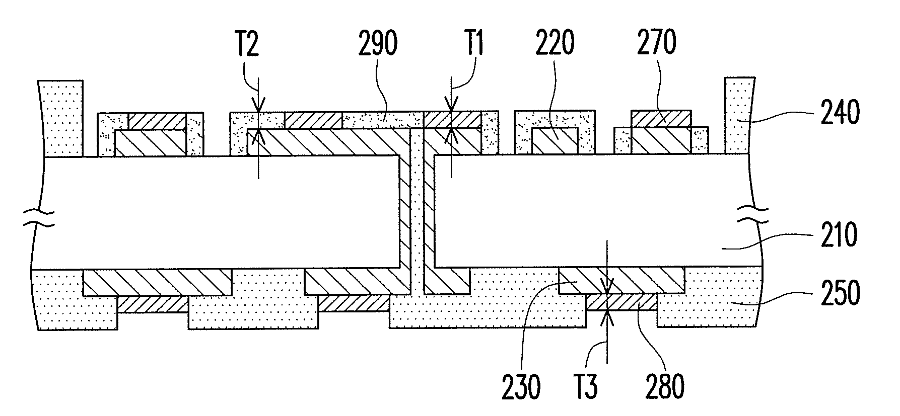
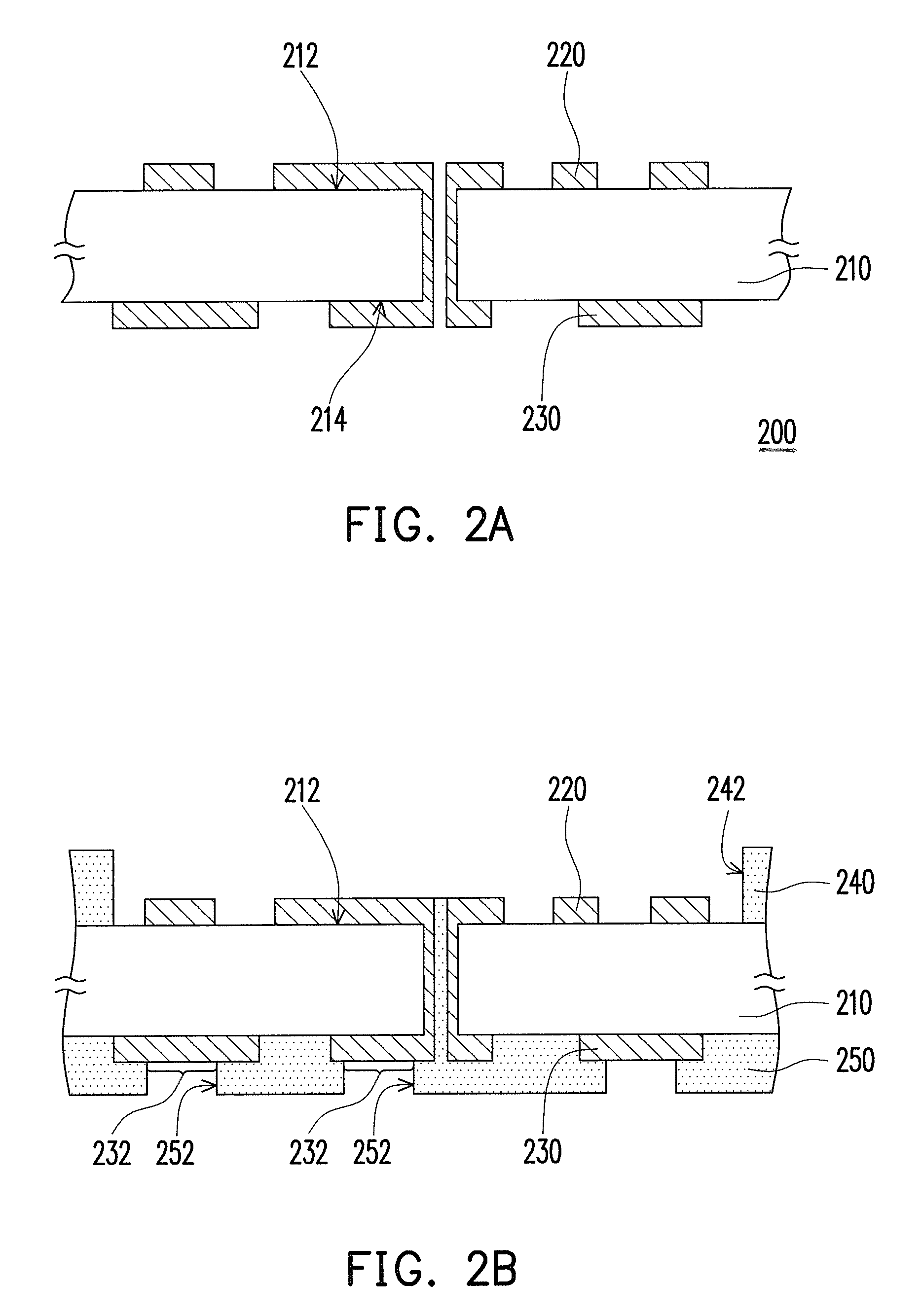
[0022]FIGS. 2A to 2F show a surface treatment process for a circuit board according to an embodiment of the present invention. First, referring to FIG. 2A, the circuit board 200 includes a substrate 210, a first circuit layer 220, and a second circuit layer 230. The substrate 210 includes a first surface 212 and a second surface 214, and the first surface 212 is reverse to the second surface 214. The first circuit layer 220 is disposed on the first surface 212, and the second circuit layer 230 is disposed on the second surface 214. The first circuit layer 220 and the second circuit layer 230 are electrically connected. The substrate 210 may be a substrate, i.e. a resin substrate, without a circuit la...


PUM

PropertyMeasurementUnit
thicknessaaaaaaaaaa
thicknessaaaaaaaaaa
thicknessaaaaaaaaaa

Abstract

A surface treatment process for a circuit board is provided. The circuit board includes a substrate, a first circuit layer disposed on an upper surface of the substrate, and a second circuit layer disposed on a lower surface of the substrate. The first circuit layer is electrically connected to the second circuit layer. In the surface treatment process for the circuit board, a first oxidation protection layer and a second oxidation protection layer are respectively formed on a portion of the first circuit layer and a portion of the second circuit layer by immersion. Afterwards, the first circuit layer exposed by the first oxidation protection layer is subjected to black oxidation to form a black oxide layer. The thickness of the first oxidation protection layer is thinner than or equal to the thickness of the black oxide layer.

Description

CROSS-REFERENCE TO RELATED APPLICATION[0001]This application claims the priority benefit of Taiwan application serial no. 97103477, filed Jan. 30, 2008. The entirety of the above-mentioned patent application is hereby incorporated by reference herein and made a part of specification.BACKGROUND OF THE INVENTION[0002]1. Field of the Invention[0003]The present invention relates to a process of a circuit board, and in particularly, relates to a surface treatment process for a circuit board.[0004]2. Description of Related Art[0005]In recent years, along with the progressive development of electronic technology and improvement of high-tech electronic industries, more humanistic electronic products with better functions are continuously put forward and progress towards “light, thin, short, and small.” Under such a trend, circuit boards having advantages of closed wiring, compact assembly, and good performance have become a main medium for carrying and electrically connecting a plurality of...

Claims


Application Information

Patent Timeline
Patent Type & Authority Applications(United States)
IPC IPC(8): H05K3/00
CPCH05K3/243H05K3/3452H05K2203/058H05K2203/0315H05K2201/2081
Inventor WANG, CHIEN-HAO
Owner ADVANCED SEMICON ENG INC
Why Eureka
Try Eureka