Method of encapsulating an electronic component

a technology of electronic components and encapsulation methods, applied in the direction of semiconductor devices, semiconductor/solid-state device details, electrical devices, etc., can solve the problem of easy damage of encapsulated components, and achieve the effect of reducing the cost of substrate use and design

Inactive Publication Date: 2009-07-30
PENG YU KANG
View PDF8 Cites 3 Cited by
  • Summary
  • Abstract
  • Description
  • Claims
  • Application Information

AI Technical Summary

Benefits of technology

[0007]In this invention, the procedure of encapsulation the electronic component is provided, in which after being encapsulated, the chip is formed and mounted with the colloid but no carrier; the costs of substrate use and design may be decreased and no consideration of heat expansion between the substrate and the chip is made.

Problems solved by technology

However, in the conventional method of encapsulation, materials are different in the coefficient of heat expansion, and thus the encapsulated component is easily damaged when being heated to cause a stress strain.

Method used


Image

  • Method of encapsulating an electronic component
  • Method of encapsulating an electronic component
  • Method of encapsulating an electronic component

Examples


Embodiment Construction

[0015]Now, the present invention will be described more specifically with reference to the following embodiments. It is to be noted that the following descriptions of preferred embodiments of this invention are presented herein for purpose of illustration and description only; it is not intended to be exhaustive or to be limited to the precise form disclosed.

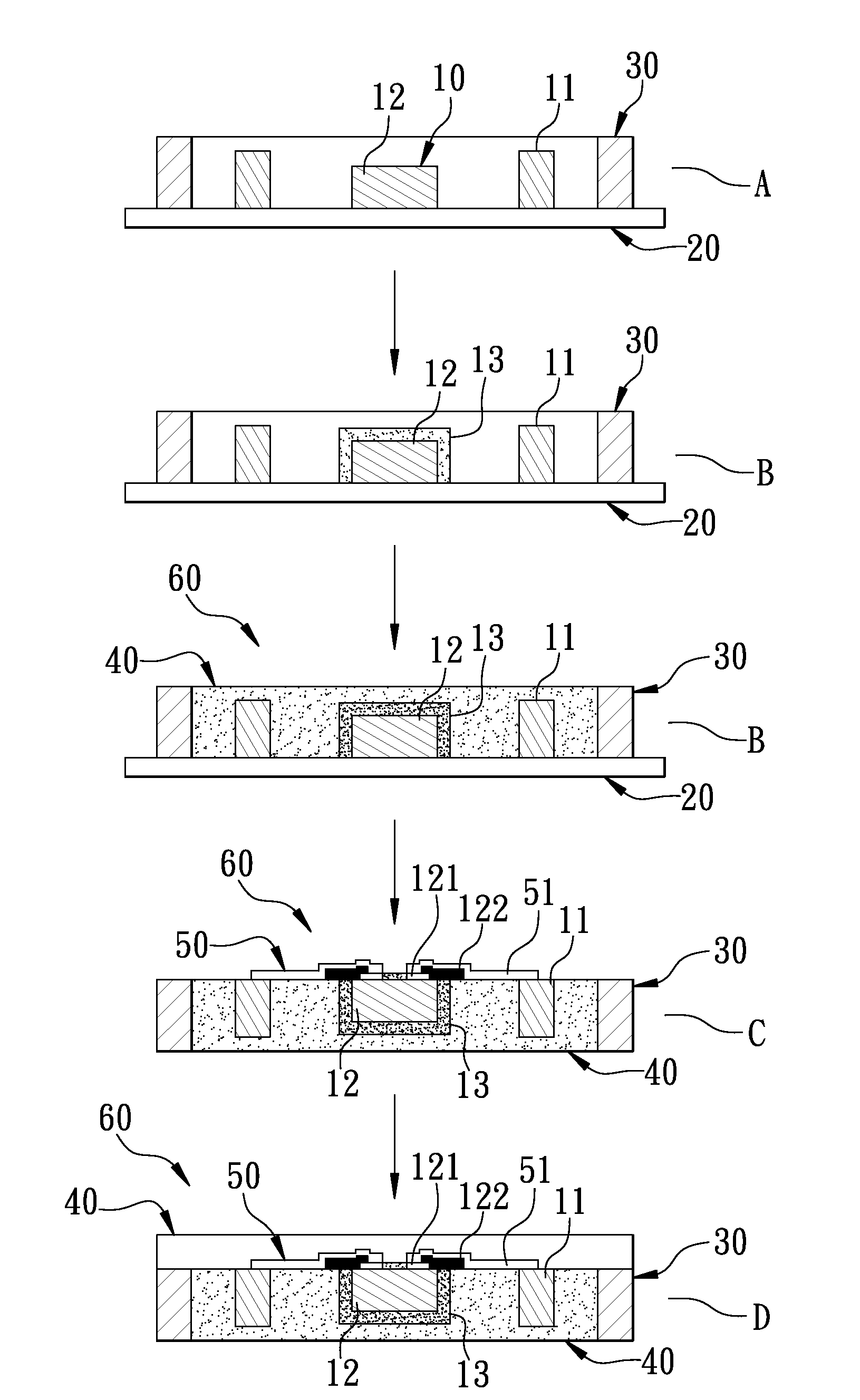
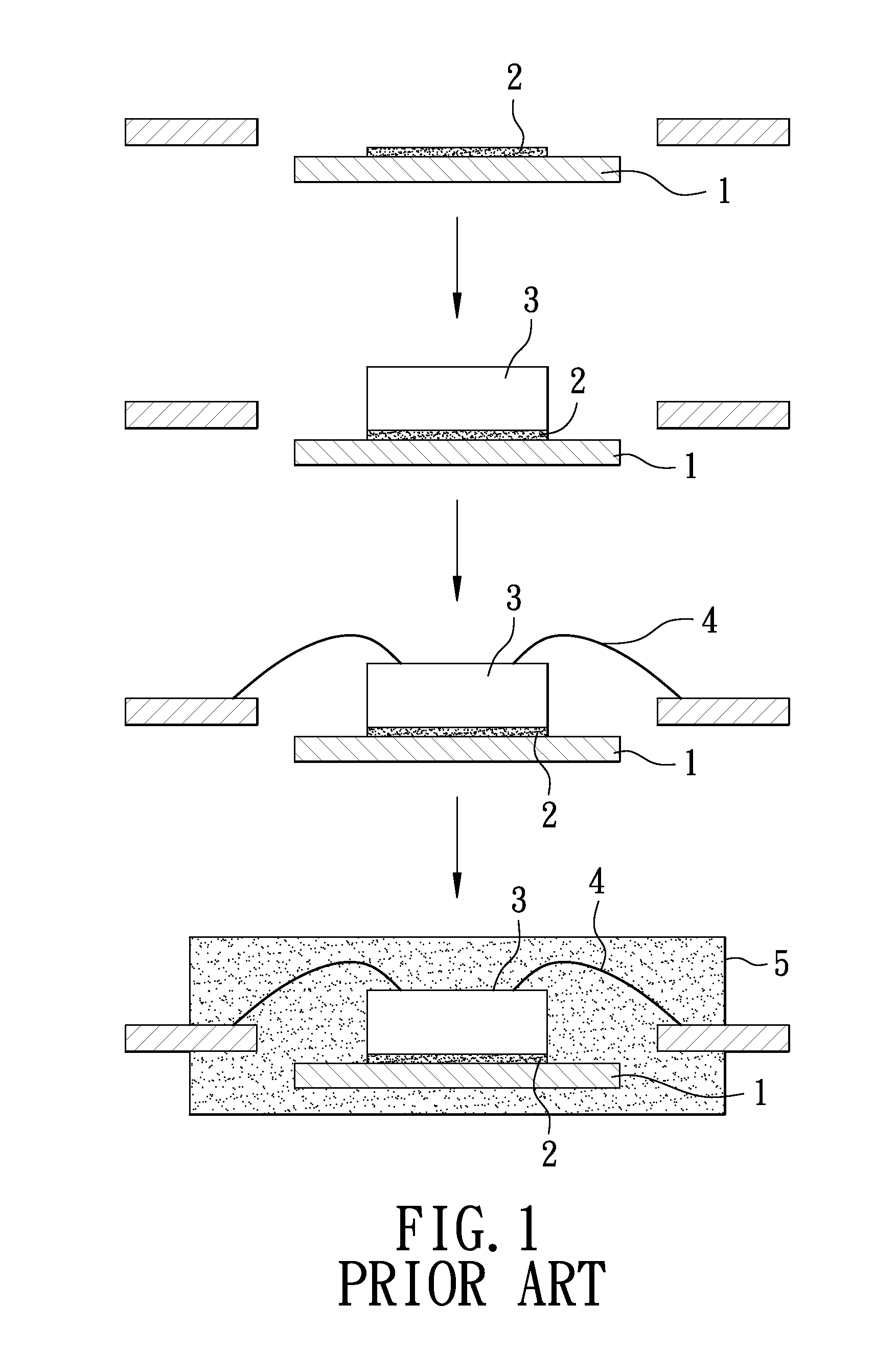
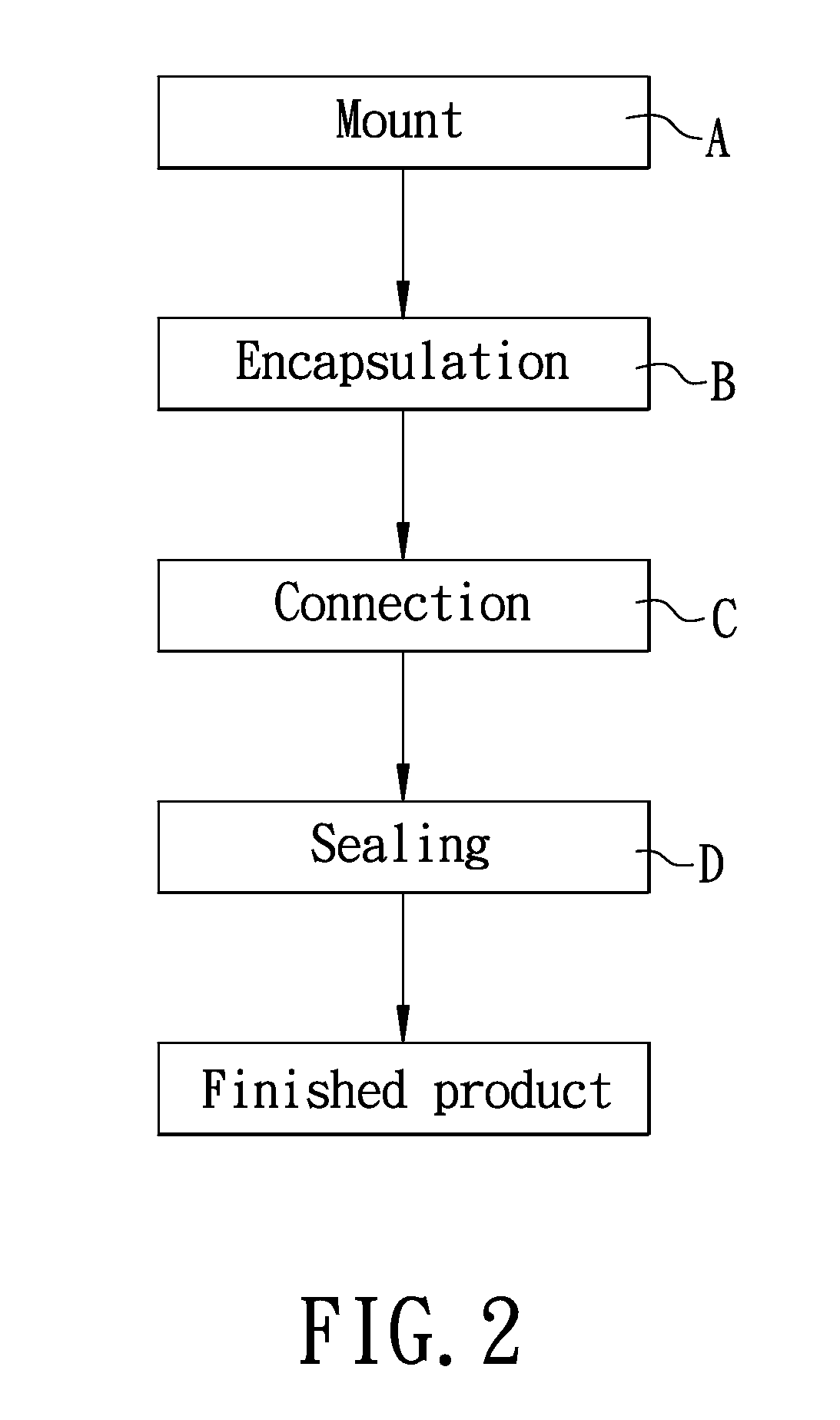
[0016]With reference to FIGS. 2 and 3 illustrating a preferred embodiment, a procedure of encapsulating an electronic component is provided in this invention, comprising the following steps.[0017]A. Mount: a chipset 10 provided with a conductor 11 and a chip 12 are temporarily mounted on a carrier 20 movable, in which the carrier 20 may be formed with an adhesive material or the conductor 11 and the chip 12 is made to be adhered onto the carrier 20 or firmly mounted on a predetermined position of the carrier 20 for fear of displacement; further, outward around the chipset 10 mounted on the carrier 20, a hollow frame 30 is provid...


PUM


Abstract

A procedure of packaging an electronic component is provided, comprising the following steps: step A for mount at which a conductor and a chip are temporarily mounted on a carrier removable, and next step B for encapsulation at which the conductor and the chip are encapsulated with colloid and mounted and then removed from the carrier so that the chipset after modeled without any substrate may be mounted for decreasing the costs of substrate use and design and the probability of damage of the substrate an chip due to the thermal expansion and increasing the yield factor of a finished product.

Description

BACKGROUND OF THE INVENTION[0001]1. Field of the Invention[0002]This invention relates to a encapsulating method and particularly to a method of encapsulating an electronic component without any substrate into a unit.[0003]2. Description of Related Art[0004]With reference to FIG. 1, in a conventional method of encapsulating a semiconductor, an adhesive resin 2 is coated on a lead frame 1, a die 3 is connected and fixed onto the lead frame 1, a bonding wire 4 is used to connect the lead frame 1 conductively to the die 3, and finally a resin 5 is used for encapsulation, thereby an integrated circuit being formed. However, in the conventional method of encapsulation, materials are different in the coefficient of heat expansion, and thus the encapsulated component is easily damaged when being heated to cause a stress strain.[0005]Consequently, because of the technical defects of described above, the applicant keeps on carving unflaggingly through wholehearted experience and research to ...

Claims


Application Information

Patent Timeline
Patent Type & Authority Applications(United States)
IPC IPC(8): H01L21/56
CPCH01L21/568H01L2924/01006H01L24/19H01L2221/68359H01L2224/04105H01L2224/20H01L2224/32245H01L2224/48091H01L2224/48247H01L2224/73265H01L2224/83192H01L2224/92H01L2224/92247H01L2924/01082H01L2924/14H01L2924/01005H01L23/3135H01L2924/00015H01L2924/181H01L2924/00014H01L2924/00012
Inventor PENG, YU-KANG
Owner PENG YU KANG
Why Eureka
Try Eureka