Thin Film Transistor Array Panel

a transistor array and thin film technology, applied in the direction of electrical equipment, semiconductor devices, instruments, etc., can solve the problems of misalignment of signal input pad and signal output pad of flexible film, change in flexible substrate size, etc., to improve junction margin and reduce process failure

Inactive Publication Date: 2009-08-20
SAMSUNG DISPLAY CO LTD
View PDF4 Cites 2 Cited by
  • Summary
  • Abstract
  • Description
  • Claims
  • Application Information

AI Technical Summary

Benefits of technology

[0010]Embodiments of the present invention provide a thin film transistor array panel that may reduce a process failure by forming a signal input pad that may improve a junction margin

Problems solved by technology

However, because a glass substrate is heavy and brittle, it is inappropriate to use the glass substrate in a display device that has a light weight, that endures some deformation, and that requires that it does not break on impact.
However, unlike a conventional glass substrate, the size of the flexible substrate may change because a flexible substrate such as a

Method used


Image

  • Thin Film Transistor Array Panel
  • Thin Film Transistor Array Panel
  • Thin Film Transistor Array Panel

Examples


Embodiment Construction

[0038]An exemplary embodiment of the present invention will be described hereinafter in detail with reference to the accompanying drawings.

[0039]In the drawings, the thickness of layers, films, panels, regions, etc., are exaggerated for clarity. Like reference numerals designate like elements throughout the specification. When it is said that any part, such as a layer, film, area, or plate, is positioned on another part, it means the part may be directly on the other part or above the other part with at least one intermediate part. In contrast, when an element is referred to as being “directly on” another element, there are no intervening elements present.

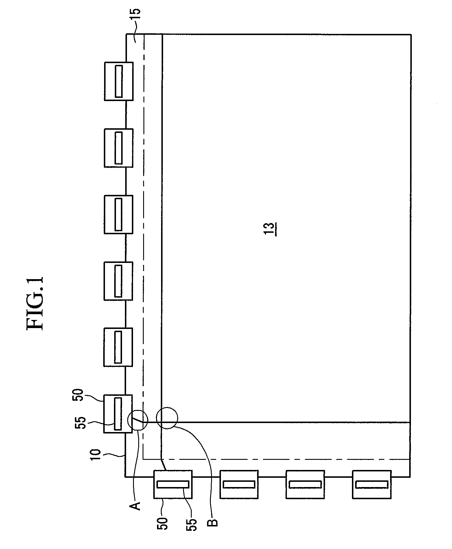
[0040]FIG. 1 is a schematic diagram of a display device according to an exemplary embodiment of the present invention.

[0041]Referring to FIG. 1, the display device includes a thin film transistor array panel 10 and a plurality of tape-carrier packages (TCP) 50.

[0042]The thin film transistor array panel 10 is partitioned into a disp...


PUM


Abstract

A thin film transistor array panel is provided according to one or more embodiments. In an embodiment, the thin film transistor array panel includes: a base substrate that has a display area and a peripheral area; a plurality of thin film transistors that are formed in the display area; a plurality of signal input pads that are formed in the peripheral area and that are formed long in a first direction; and a plurality of signal lines that are connected to the thin film transistors and the signal input pads, wherein at least a part of each of the plurality of signal input pads is arranged in a line along the first direction.

Description

CROSS-REFERENCE TO RELATED APPLICATION[0001]This application claims priority to and the benefit of Korean Patent Application No. 10-2008-0015419 filed in the Korean Intellectual Property Office on Feb. 20, 2008, the entire contents of which are incorporated herein by reference.BACKGROUND[0002](a) Technical Field[0003]Embodiments of the present invention generally relate to a thin film transistor array panel.[0004](b) Description of the Related Art[0005]In a thin film transistor array panel that is used in a general display device, a plurality of gate lines and a plurality of data lines are formed to intersect each other, a pixel electrode and a thin film transistor, which is a switching element, are formed in an intersecting region of the gate line and the data line, and signal input pads that are electrically connected to a driving device are formed at one end of each of the gate line and the data line. The driving device is mounted in a flexible circuit layer in an integrated circ...

Claims


Application Information

Patent Timeline
IPC IPC(8): H01L29/04
CPCH01L27/124H01L29/78603G02F1/13458G02F1/136286H01L27/1214
Inventor LEE, SON-UKKIM, SUNG-JINLEE, JEONG-KUK
Owner SAMSUNG DISPLAY CO LTD
Why Eureka
Try Eureka