Method of manufacturing a buried-gate semiconductor device and corresponding integrated circuit

Active Publication Date: 2009-08-27
COMMISSARIAT A LENERGIE ATOMIQUE ET AUX ENERGIES ALTERNATIVES +1
View PDF14 Cites 4 Cited by
  • Summary
  • Abstract
  • Description
  • Claims
  • Application Information

AI Technical Summary

Benefits of technology

[0027]Advantageously, the alloy of the first material and of the second semiconductor material comprises a relative proportio

Problems solved by technology

It is recalled here that a short channel has a very short distance (length) between the source and the drain and that the “short-channel” effect results in a reduction of the threshold voltage of the transistor, which can, at the extreme limit, result in obtaining a transistor that is very difficult to control and can finish up in the “piercing” mode.
However, with the reduction of the dimensions for forthcoming semiconductor devices, a gat

Method used


Image

  • Method of manufacturing a buried-gate semiconductor device and corresponding integrated circuit
  • Method of manufacturing a buried-gate semiconductor device and corresponding integrated circuit
  • Method of manufacturing a buried-gate semiconductor device and corresponding integrated circuit

Examples


Example

DETAILED DESCRIPTION OF THE DRAWINGS

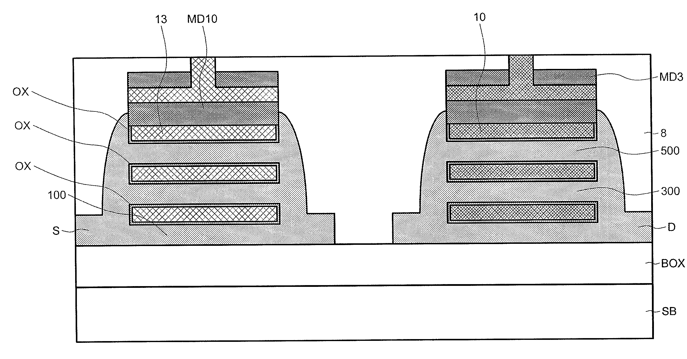
[0035]There is described here, by way of example, a method for manufacturing a transistor with a surrounding gate comprising for example three semiconductor channel regions, two of which are surrounded by the gate region.

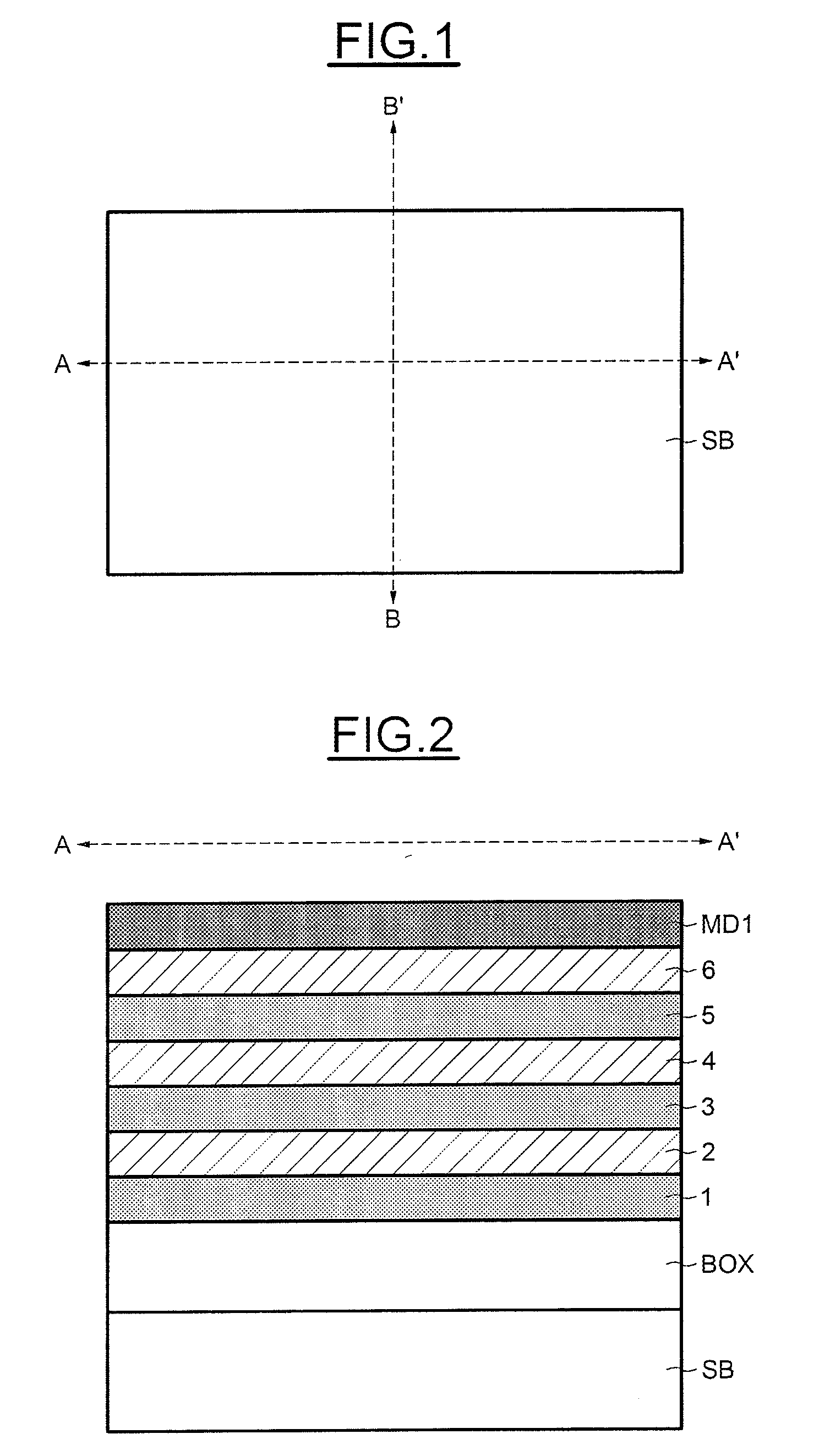
[0036]In FIG. 1, the reference SB indicates a semiconductor wafer or semiconductor substrate that has been shown here in plan view in a rectangular shape for purposes of simplification.

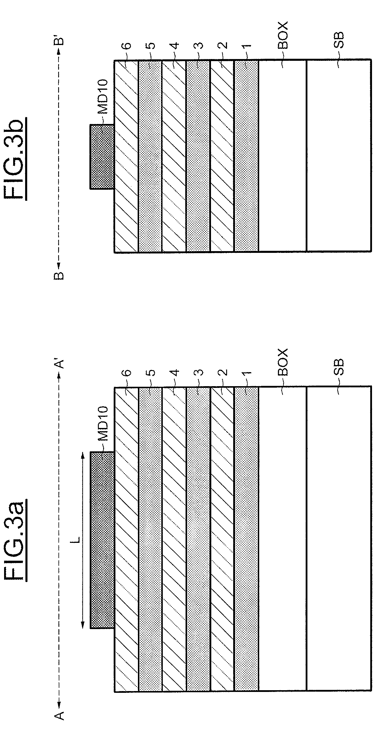
[0037]In the rest of the FIGURES, those which are numbered with the letter “a” correspond to a cross-sectional view in the direction AA′ of FIG. 1, while those which are numbered with the letter “b” correspond to a cross-sectional view in the general direction BB′.

[0038]The first phase of the method comprises, as shown in FIG. 2, in forming on the substrate SB an insulating base layer (buried oxide) BOX surmounted by a stack formed from a first layer of silicon 1, a second layer of silicon 3 encapsulated between two sacrificial layers 2 and 4, and a...


PUM


Abstract

A semiconductor device includes a semiconductor channel region and a gate region, wherein the gate region includes at least one buried part extending under the channel region. The buried part of the gate region is formed from a cavity under the channel region. The cavity is filled with a first material. An opening is made to access the first material. In one implementation, aluminum is deposited in the opening in contact with the first material. An anneal is performed to cause the aluminum to be substituted for the first material in the cavity. In another implementation, a second material different from the first material is deposited in the opening. An anneal is performed to cause an alloy of the first and second materials to be formed in the cavity.

Description

PRIORITY CLAIM[0001]The present application is a translation of and claims priority from French Application for Patent No. 08 51265 of the same title filed Feb. 27, 2008, the disclosure of which is hereby incorporated by reference.BACKGROUND OF THE INVENTION[0002]1. Technical Field of the Invention[0003]The present invention relates to integrated circuits, and more particularly to buried-gate semiconductor devices, that is to say those of which at least a portion of the gate region is placed below the channel region.[0004]2. Description of Related Art[0005]Among the semiconductor devices with so-called buried gates are distinguished devices with a double planar gate, that it so say in which the gate region comprises two gates, one of which is situated above the channel region and the other of which is situated below the channel region, and the so-called GAA (Gate All Around) devices in which the gate region is formed from a single part and surrounds the channel region.[0006]Buried-g...

Claims


Application Information

Patent Timeline
IPC IPC(8): H01L29/78H01L21/4763H01L21/36H01L21/336
CPCH01L29/42392H01L29/78696H01L29/66787H01L29/4908
Inventor BERNARD, EMILIEGUILLAUMOT, BERNARDCORONEL, PHILIPPEVIZIOZ, CHRISTIAN
Owner COMMISSARIAT A LENERGIE ATOMIQUE ET AUX ENERGIES ALTERNATIVES
Why Eureka
Try Eureka