Frame pulse signal latch circuit and phase adjustment method

a latch circuit and frame pulse technology, applied in the direction of pulse technique, generating/distributing signals, instruments, etc., can solve the problems of long adjustment time, process carried out, and the latch circuit cannot generate the original frame pulse signal

Inactive Publication Date: 2009-08-27
NEC CORP
View PDF4 Cites 2 Cited by
  • Summary
  • Abstract
  • Description
  • Claims
  • Application Information

AI Technical Summary

Problems solved by technology

In this case, the latch circuit can no longer generate the frame pulse signal having the original cycle.
However, in the conventional adjustment methods, the process carried out until an optimal phase point is found is complicated, and long time is taken for adjustment as a result, which is a problem.
Moreover, since the optimal phase point has been sensuously determined by judgment of engineers, automating the

Method used


Image

  • Frame pulse signal latch circuit and phase adjustment method
  • Frame pulse signal latch circuit and phase adjustment method
  • Frame pulse signal latch circuit and phase adjustment method

Examples


first embodiment

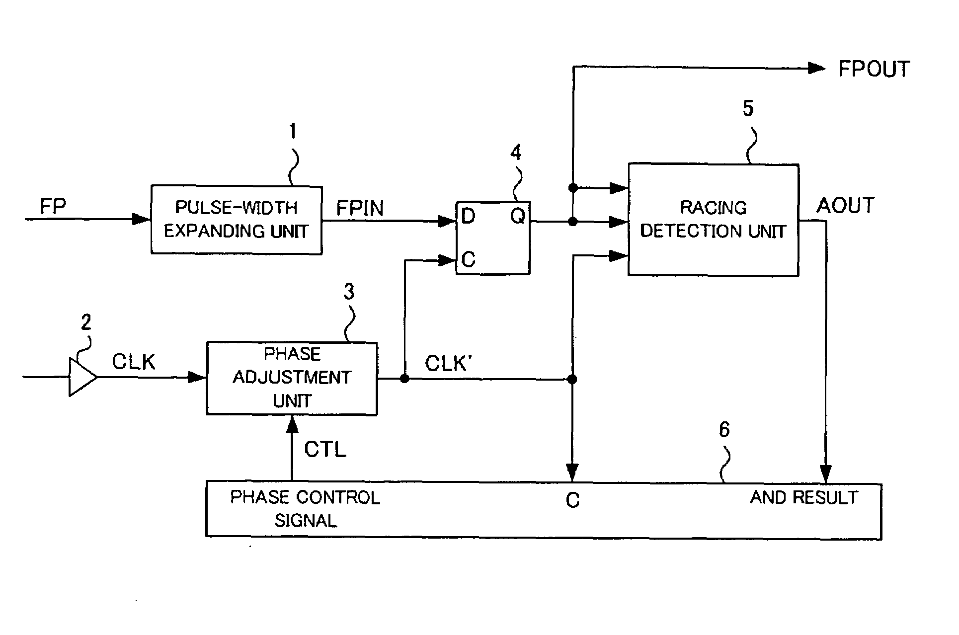
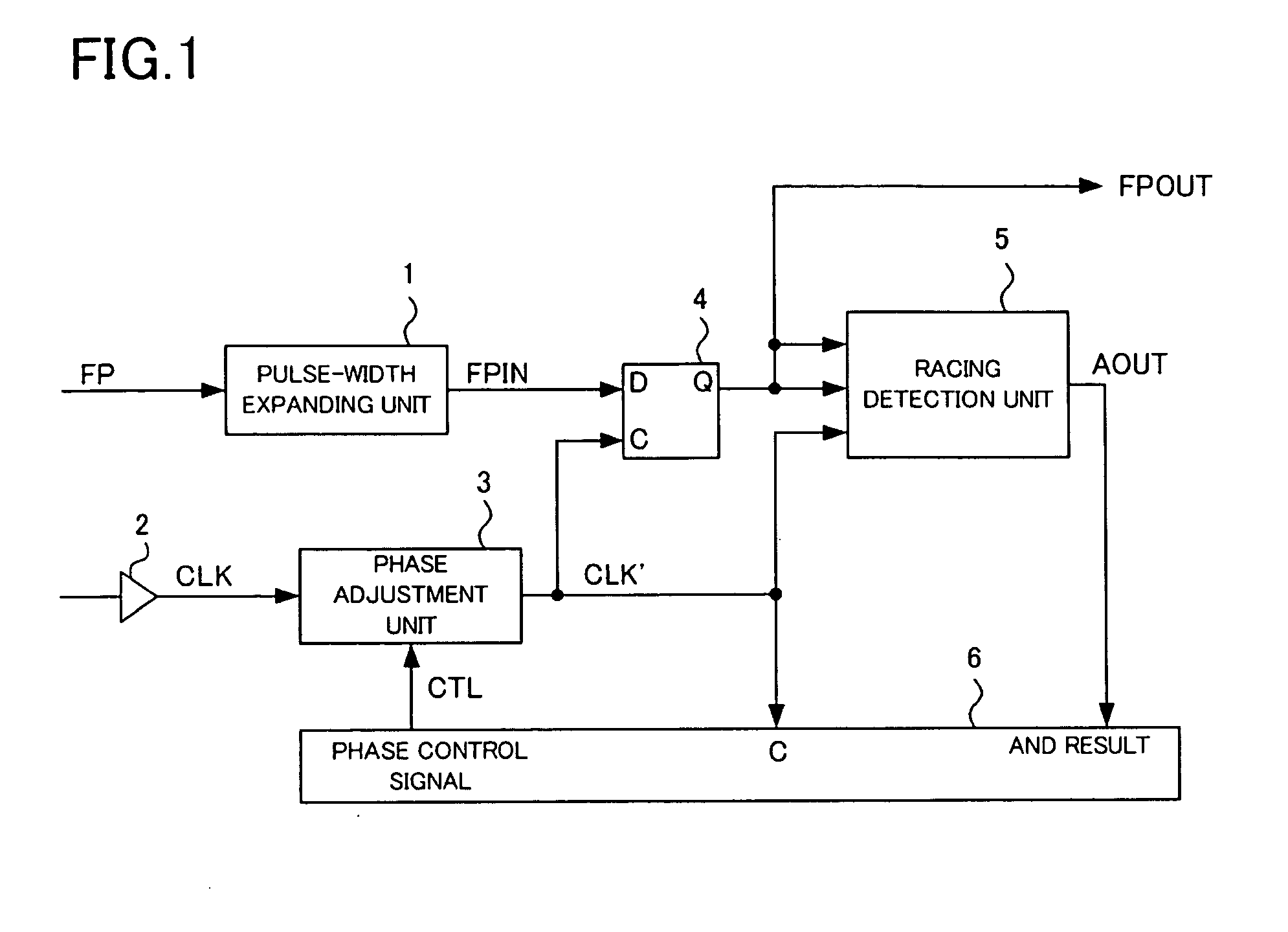
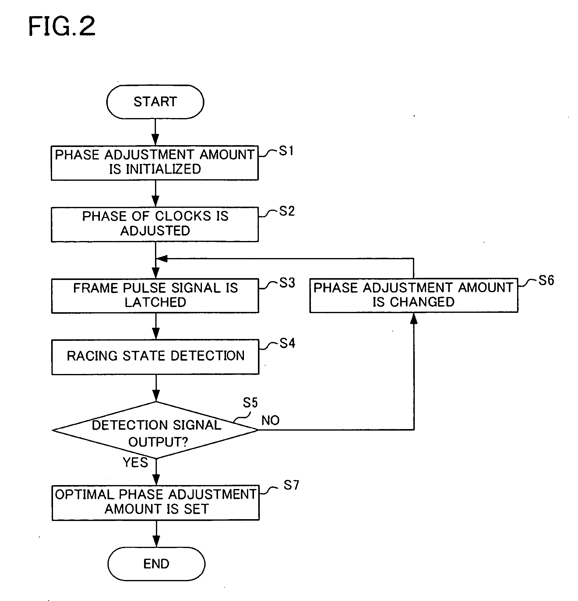
[0036]Hereinafter, embodiments of the present invention will be explained with reference to drawings. FIG. 1 is a block diagram showing a configuration of a frame pulse signal latch circuit according to a first embodiment of the present invention.

[0037]The frame pulse signal latch circuit of the present embodiment has a pulse-width expanding unit 1, a buffer 2, a phase adjustment unit 3, a flip-flop 4, a racing detection unit 5, and a control unit 6.

[0038]The pulse-width expanding unit 1 receives an input frame pulse signal FP, which has a pulse width of an m (m is a positive integer)-clock cycle, from a transmitting side and outputs a frame pulse signal FPIN which is obtained by extending the pulse width of the frame pulse signal FP to be longer than the m-clock cycle.

[0039]The buffer 2 receives clocks from the transmitting side.

[0040]The phase adjustment unit 3 generates output clocks CLK′, which are obtained by adjusting the phase of input clocks CLK based on a directed phase adj...

second embodiment

[0057]Next, a second embodiment of the present invention will be explained. FIG. 3 is a block diagram showing a configuration of a frame pulse signal latch circuit according to the second embodiment of the present invention. The present embodiment explains the first embodiment in more detail. In the present embodiment, the pulse width of the frame pulse signal FP is a one-clock cycle.

[0058]The frame pulse signal latch circuit of the present embodiment has buffers 10 and 11, a PLL circuit 12, a flip-flop 13, a flip-flop 14, an AND circuit 15, and a control circuit 16.

[0059]The buffer 10 functions as the pulse-width expanding unit, which receives the frame pulse signal FP from the transmitting side. The buffer 11 receives clocks from the transmitting side.

[0060]The PLL circuit 12 functions as the phase adjustment unit which adjusts the phase of the clocks CLK output from the buffer 11 and outputs the clocks CLK′ which has been phase-adjusted.

[0061]The flip-flop 13 functions as the lat...

third embodiment

[0083]Next, a third embodiment of the present invention will be explained. FIG. 8 is a block diagram showing a configuration of a frame pulse signal latch circuit according to the third embodiment of the present invention. Note that constituents similar to the constituents shown in FIG. 3 are denoted by the same reference numerals. In the present embodiment, the pulse width of the frame pulse signal FP is a two-clock cycle.

[0084]The frame pulse signal latch circuit of the present embodiment has the buffers 10 and 11, the PLL circuit 12, the flip-flops 13, 14, and 17, an AND circuit 15a, and the control circuit 16.

[0085]The buffer 10 receives the frame pulse signal FP from the transmitting side. The buffer 11 receives clocks from the transmitting side.

[0086]The PLL circuit 12 adjusts the phase of the clocks CLK, which is output from the buffer 11, and outputs the adjusted clocks CLK′.

[0087]The flip-flop 13 latches the frame pulse signal FPIN, which is output from the buffer 10, in sy...


PUM


Abstract

A frame pulse signal latch circuit has: a pulse-width expanding unit which outputs a frame pulse signal FPIN having a pulse width longer than a m-clock cycle; a phase adjustment unit which generates a phase-adjusted output clock CLK′; a flip-flop which latches the frame pulse signal FPIN; a racing detection unit which generates signals, which are shifted by one to m clocks with respect to a frame pulse signal FPOUT, and detects a racing state based on a result of an AND operation of the frame pulse signal FPOUT and the clock-shifted signals; and a control unit which sequentially selects and directs different phase adjustment amounts to the phase adjustment unit, determines an optimal phase adjustment amount based on a worst phase adjustment amount of the case in which the racing state is detected, and gives a direction about the optimal phase adjustment amount to the phase adjustment unit.

Description

[0001]This application is based on Japanese Patent Application No. 2008-044017 filed on Feb. 26, 2008 and including specification, claims, drawings and summary. The disclosure of the above Japanese Patent Application is incorporated herein by reference in its entirety.BACKGROUND OF THE INVENTION[0002]1. Field of the Invention[0003]The present invention relates to a frame pulse signal latch circuit which latches a frame pulse signal repeatedly transmitted at a constant pulse width and, in particular, to a frame pulse signal latch circuit and a phase adjustment method readily enabling evaluation and adjustment of latch timing.[0004]2. Description of the Related Art[0005]Along with increase of the integration degree and the processing speed of an electronic circuit, the frequency of a system clock used in control of the electronic circuit is increasing. Accordingly, when digital signals are to be transferred between printed wiring boards or devices, the permissible errors about the pha...

Claims


Application Information

Patent Timeline
IPC IPC(8): H03K5/04
CPCH03K5/05
Inventor TAKAHASHI, TSUGIO
Owner NEC CORP
Why Eureka
Try Eureka