Display device

a technology of display panel and liquid crystal display, which is applied in the direction of static indicating devices, instruments, etc., can solve the problems of high power consumption during operation, complicated structure of each pixel, and difficulty in directly connecting such a liquid crystal display panel to a microcomputer or the like, so as to reduce power consumption, simplify the structure of the pixel, and improve the effect of operation speed

Inactive Publication Date: 2009-08-27
PANASONIC LIQUID CRYSTAL DISPLAY CO LTD +1
View PDF2 Cites 1 Cited by
  • Summary
  • Abstract
  • Description
  • Claims
  • Application Information

AI Technical Summary

Benefits of technology

[0023]With the display device having such a structure, the structure of the pixel can be simplified, the operation speed can be improved, and the power consumption can be reduced.

Problems solved by technology

It is difficult to directly connect such a liquid crystal display panel to a microcomputer or the like.
However, because the liquid crystal display panel of FIG. 6 uses the Y-address circuit YAD and the X-address circuit XAD, the structure of each pixel becomes more complicated, and thus such a structure is disadvantageous when the number of bits is to be increased.
In addition, the Y-address circuit YAD and the X-address circuit XAD have a slower operation speed compared to, for example, a shift register in the RGB interface, and there is also a disadvantage that the power consumption during operation is higher.

Method used


Image

  • Display device
  • Display device
  • Display device

Examples


Embodiment Construction

[0030]A display device according to a preferred embodiment of the present invention will now be described with reference to the drawings.

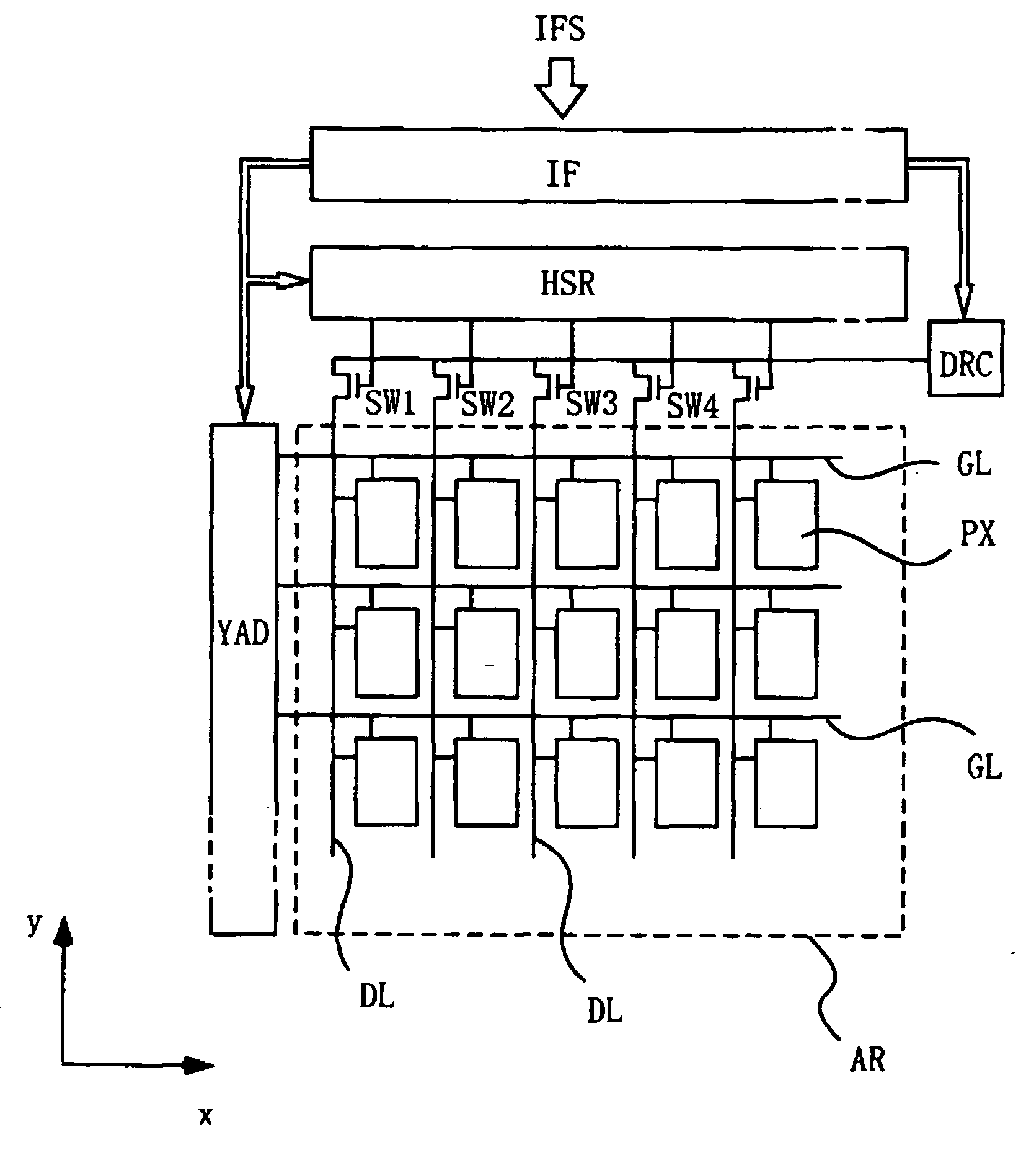
[0031]FIG. 1 is a schematic structural diagram showing an example of a display device according to a preferred embodiment of the present invention. FIG. 1 exemplifies a liquid crystal display device.

[0032]An equivalent circuit shown in FIG. 1 is formed on a substrate which forms an outer device of a liquid crystal display device (liquid crystal display panel) and which is made of, for example, glass.

[0033]A display area AR of the liquid crystal display device is formed on a surface of the substrate and a plurality of pixels PX are disposed and formed in a matrix form in the display area AR of the liquid crystal display device.

[0034]Each of scan lines GL is provided common to the pixels PX arranged along the row direction (x direction in FIG. 1). A scan signal is supplied from each of the scan lines GL to the pixels. Each of image lines DL is provid...


PUM


Abstract

A display device is provided comprising a plurality of pixels disposed in a matrix form in a display area of a substrate, each of the plurality of pixels having a memory which stores written data, a scan line which is provided common to pixels arranged along a row direction and through which a scan signal is supplied to the pixels, and an image line which is provided common to pixels arranged along a column direction and through which an image signal is supplied to the pixels, wherein the scan signal is supplied to the scan line through a vertical address circuit or a vertical shift register circuit, and data is supplied to the image line through a horizontal scan shift register circuit.

Description

CROSS-REFERENCE TO RELATED APPLICATIONS[0001]The present application claims priority from Japanese application JP 2008-043794A filed on Feb. 26, 2008, the content of which is hereby incorporated by reference into this application.BACKGROUND OF THE INVENTION[0002]1. Field of the Invention[0003]The present invention relates to a display device, and, in particular, to a display device having a memory in each pixel in a display area.[0004]2. Description of the Related Art[0005]A display device is discloses in, for example, JP 2006-285118 A in which a memory is provided in each pixel in a display area of a liquid crystal display panel and display data is stored in the memory so that an image is displayed on the liquid crystal display panel even when there is no input data from the outside.[0006]FIG. 5 is a diagram schematically showing a structure of such a liquid crystal display panel. The liquid crystal display panel comprises pixels PX disposed in a display area AR of the liquid cryst...

Claims


Application Information

Patent Timeline
Patent Type & Authority Applications(United States)
IPC IPC(8): G09G3/36
CPCG09G3/2096G09G3/3607G09G2330/022G09G3/3677G09G3/3648
Inventor YASUDA, KOZO
Owner PANASONIC LIQUID CRYSTAL DISPLAY CO LTD
Why Eureka
Try Eureka