Pixel for organic light emitting diode display and OLED display

a light-emitting diode and pixel technology, applied in the direction of electrical equipment, semiconductor devices, instruments, etc., can solve the problems of uniform electrical characteristics of the pixel, and achieve the effect of simplifying the pixel structure and increasing driving reliability

Active Publication Date: 2020-07-02
LG DISPLAY CO LTD
View PDF4 Cites 0 Cited by
  • Summary
  • Abstract
  • Description
  • Claims
  • Application Information

AI Technical Summary

Benefits of technology

[0008]The present disclosure provides a pixel for an organic light emitting diode (OLED) display and an OLED display including a pixel circuit capable of simplifying a pixel structure and increasing driving reliability.

Problems solved by technology

Driving transistors disposed in all pixels should have the same electrical characteristics, but their electrical characteristics are not uniform due to the process conditions or a driving environment, etc.

Method used


Image

  • Pixel for organic light emitting diode display and OLED display
  • Pixel for organic light emitting diode display and OLED display
  • Pixel for organic light emitting diode display and OLED display

Examples


first embodiment

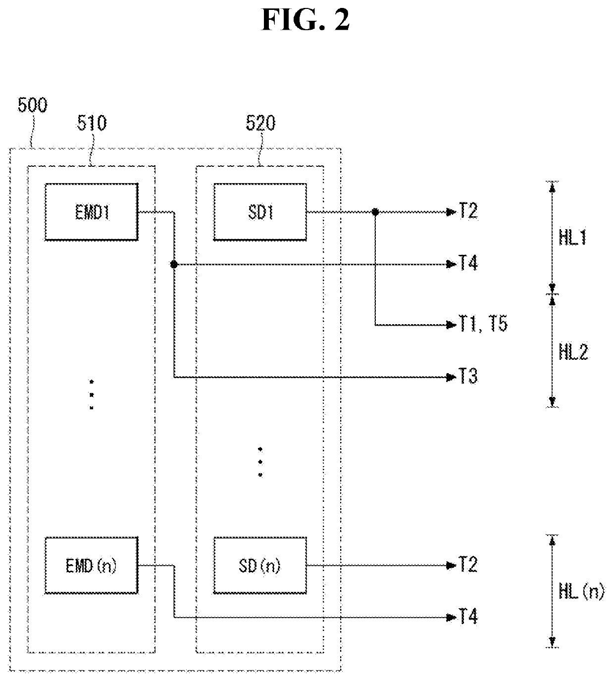
[0034]Referring to FIGS. 2 and 3, the shift register 500 includes an emission signal generator 510 and a scan signal generator 520. First to n-th emission drivers EMD1 to EMD(n) of the emission signal generator 510 are connected to each other in cascade, and first to n-th scan drivers SD1 to SD(n) of the scan signal generator 520 are connected to each other in cascade.

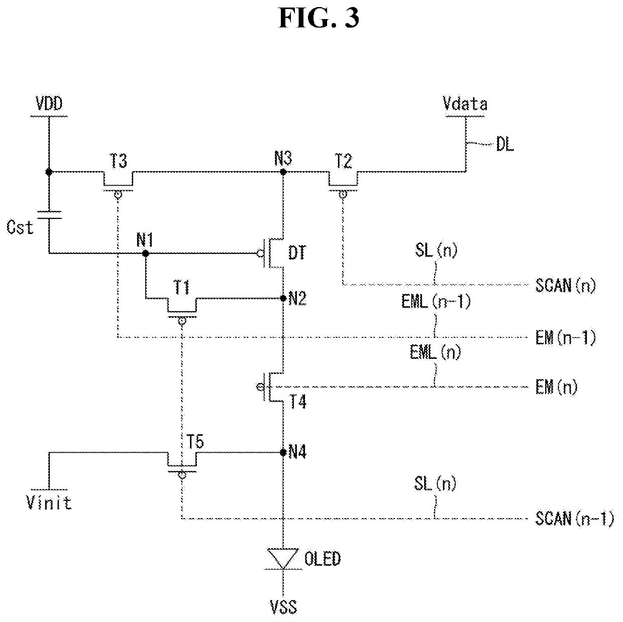
[0035]The emission signal generator 510 includes the first to n-th emission drivers EMD1 to EMD(n). The first emission driver EMD1 generates an emission signal EM1 and applies the emission signal EM1 to a first emission control transistor T4 of a first pixel line HL1 and a second emission control transistor T3 of a second pixel line HL2. The n-th emission driver EMD(n) generates an emission signal EM(n) and applies the emission signal EM(n) to a first emission control transistor T4 of an n-th pixel line HL(n).

[0036]The scan signal generator 520 includes the first to n-th scan drivers SD1 to SD(n). The first scan drive...

second embodiment

[0067]FIG. 9 illustrates a shift register according to the present disclosure. The shift register of FIG. 9 can be utilized as the shift register 500 in FIG. 1.

[0068]Referring to FIG. 9, a shift register 500 according to the second embodiment includes an emission signal generator 510 and a scan signal generator 520. First to n-th emission drivers EMD1 to EMD(n) of the emission signal generator 510 are cascade-connected to each other, and first to n-th scan drivers SD1 to SD(n) of the scan signal generator 520 are cascade-connected to each other.

[0069]The emission signal generator 510 includes the first to n-th emission drivers EMD1 to EMD(n). The first emission driver EMD1 generates an emission signal EM1 and applies the emission signal EM1 to a fourth transistor T4 and a third transistor T3 of a first pixel line HL1. The n-th emission driver EMD(n) generates an emission signal EM(n) and applies the emission signal EM(n) to a fourth transistor T4 and a third transistor T3 of an n-th...

third embodiment

[0078]FIG. 11 illustrates a shift register according to the present disclosure. The shift register of FIG. 11 can be used as the shift register 500 of FIG. 1.

[0079]Referring to FIG. 11, a shift register 500 according to the third embodiment includes an emission signal generator 510 and a scan signal generator 520.

[0080]First to n-th emission drivers EMD1 to EMD(n) of the emission signal generator 510 are cascade-connected to each other. The first emission driver EMD1 generates an emission signal EM1 and applies the emission signal EM1 to a fourth transistor T4 of a first pixel line HL1 and a third transistor T3 of a second pixel line HL2. The n-th emission driver EMD(n) generates an emission signal EM(n) and applies the emission signal EM(n) to a fourth transistor T4 of an n-th pixel line HL(n).

[0081]The scan signal generator 520 includes a scanl generator and a scan2 generator. The scanl generator includes first to n-th scanl drivers SD1(1) to SD1(n) that are cascade-connected to e...


PUM

PropertyMeasurementUnit
voltageaaaaaaaaaa
potential driving voltageaaaaaaaaaa
initialization voltageaaaaaaaaaa

Abstract

A pixel for an organic light emitting diode (OLED) display and an OLED display are discussed. The pixel includes a driving transistor, a first transistor, a scan transistor, a first emission control transistor, and an initialization control transistor. The driving transistor includes a gate electrode connected to a first node, a drain electrode connected to a second node, and a source electrode connected to a third node. The first transistor is connected between the first node and the second node. The scan transistor is connected between the third node and a data line. The first emission control transistor is connected between the second node and an anode electrode of an organic light emitting diode. The initialization control transistor is connected between an input terminal of an initialization voltage and the anode electrode of the organic light emitting diode.

Description

CROSS-REFERENCE TO RELATED APPLICATION[0001]This application claims the priority benefit of the Korean Patent Application No. 10-2018-0171836 filed on Dec. 28, 2018, the entire contents of which is incorporated herein by reference for all purposes as if fully set forth herein.BACKGROUND OF THE INVENTIONTechnical Field[0002]The present disclosure relates to a pixel for an organic light emitting diode (OLED) display and an OLED display.Related Art[0003]Flat panel displays (FPDs) have been widely used in a monitor of a mobile computer, such as a notebook computer and a tablet PC, and a mobile phone as well as a monitor of a desktop computer due to the characteristics advantageous for small-sized and light devices. Examples of the flat panel display include a liquid crystal display (LCD), a plasma display panel (PDP), a field emission display (FED), and an organic light emitting diode (OLED) display.[0004]Among the flat panel displays, the OLED display has advantages of a fast response ...

Claims


Application Information

Patent Timeline
Patent Type & Authority Applications(United States)
IPC IPC(8): G09G3/3291G09G3/3266G09G3/3225H01L27/32
CPCG09G2310/0286G09G2310/08G09G2310/0289G09G2320/0233G09G3/3266G09G2300/043H01L27/3262G09G3/3225G09G3/3291G09G3/3233G09G2300/0426G09G2320/0219G09G2300/0842G09G2300/0819G09G2300/0861G09G2320/045H10K59/1213
Inventor PARK, JONGMINPARK, DONGWONKWON, YONGCHUL
Owner LG DISPLAY CO LTD
Why Eureka
Try Eureka