Method for detecting photoelectric conversion amount and photoelectric converter, method for inputting image and device for inputting image, two-dimesional image sensor and method for driving two-dimensional image sensor

a technology of conversion amount and conversion amount, applied in the field of photoelectric converters, can solve the problems of reducing the speed of reading images, unable to reduce the size and weight of apparatus as desired, and none of them have not yet been used in practical applications, so as to reduce the size of photosensors, simplify the pixel structure, and improve the effect of resolution

Inactive Publication Date: 2005-10-13
SHARP KK
View PDF2 Cites 7 Cited by
  • Summary
  • Abstract
  • Description
  • Claims
  • Application Information

AI Technical Summary

Benefits of technology

[0020] Moreover, with the structure wherein the auxiliary capacitance is connected to the drain electrode of the thin film transistor, it is possible to manufacture the photosensor by utilizing the manufacturing process of the thin film transistor.
[0021] As described, by simplifying the pixel structure which constitutes a photosensor, it is possible to reduce the size of the photosensor. As a result, a higher resolution can be realized. Moreover, the simplified pixel structure of the photosensor also permits the manufacturing process of the photoelectric converter adopting the photosensor to be simplified.

Problems solved by technology

A problem therefore arises in that the speed of reading images is lowered, or the apparatus cannot be reduced in size and weight as desired.
For the described beneficial features which realize high speed image reading, lighter weight, thinner structure without requiring mechanical scanning, various types of close coupling two-dimensional image sensors have been proposed, but none of them have not yet been used in practical applications.
Essential factors which hinder the practical applications of the foregoing close coupling image sensor include the complex structure of the pixel and the array.
Specifically, to fabricate a photosensor, a larger number of processes are needed, or the pixel of more complicated structure is needed, or a larger pixel area is required as compared to the case of fabricating the TFT array adopted in the active matrix liquid crystal array subjected to mass production, and a higher resolution is therefore difficult to be realized.

Method used


Image

  • Method for detecting photoelectric conversion amount and photoelectric converter, method for inputting image and device for inputting image, two-dimesional image sensor and method for driving two-dimensional image sensor
  • Method for detecting photoelectric conversion amount and photoelectric converter, method for inputting image and device for inputting image, two-dimesional image sensor and method for driving two-dimensional image sensor
  • Method for detecting photoelectric conversion amount and photoelectric converter, method for inputting image and device for inputting image, two-dimesional image sensor and method for driving two-dimensional image sensor

Examples


first embodiment

[0109] The following descriptions will explain one embodiment of the present invention.

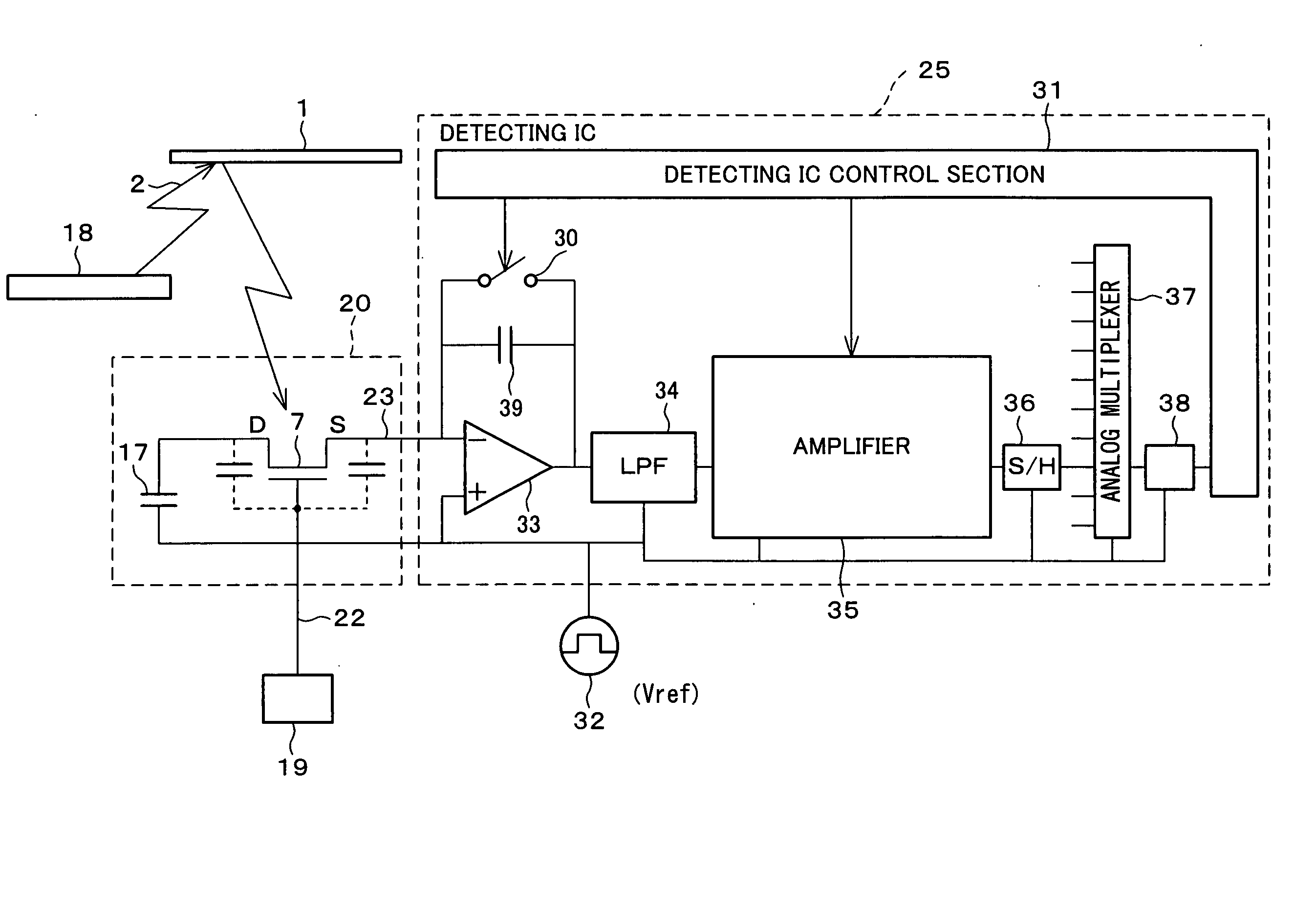
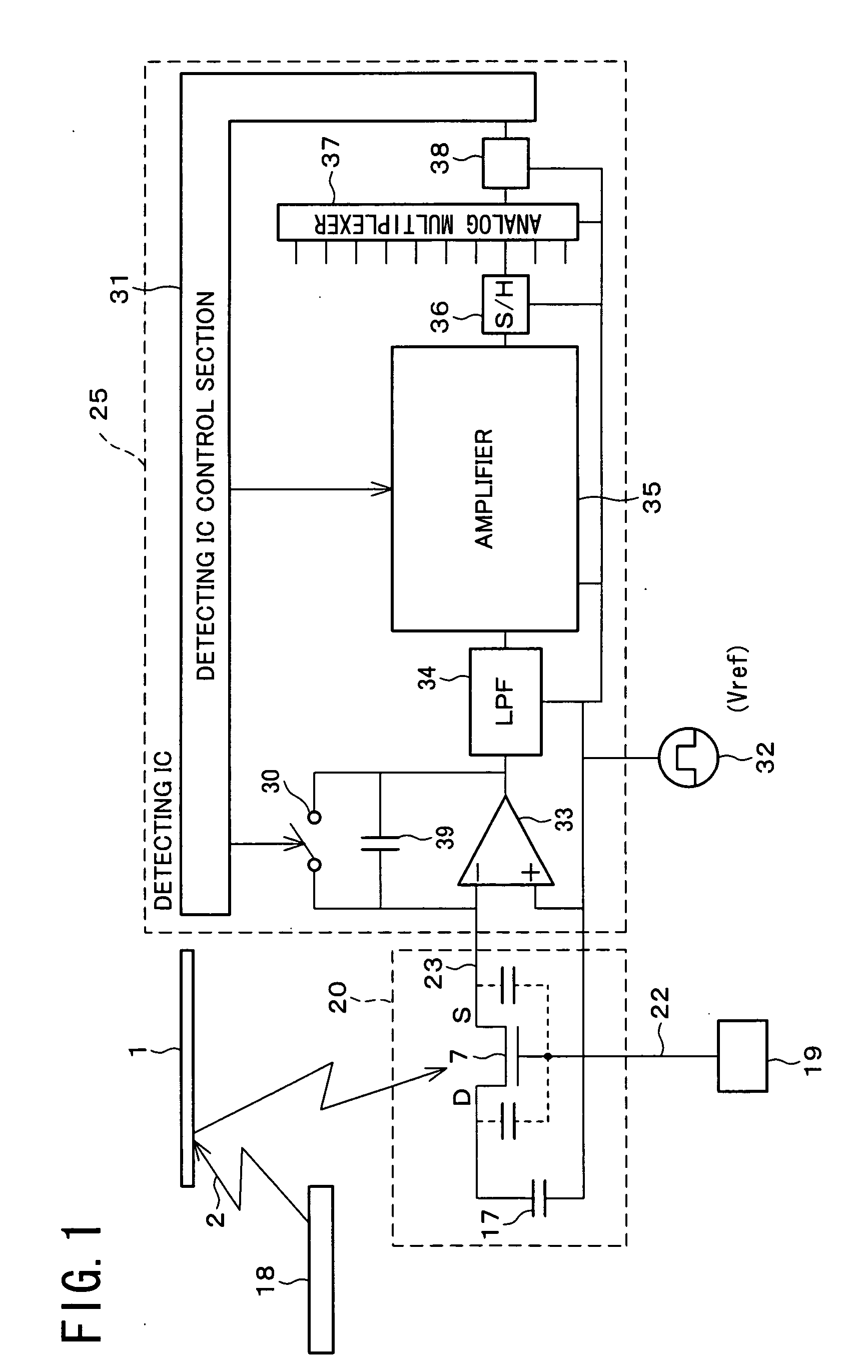
[0110] Before explaining a method for detecting a photoelectric conversion amount, a photosensor applicable to a photoelectric converter of the present invention and a two-dimensional image sensor adopting the photosensor will be explained.

[0111] The photosensor basically has the structure of the inverse stagger type thin film transistor (TFT) (Here, the stagger type thin film transistor may be adopted, provided that an upper gate electrode is made of a transparent material). Specifically, as illustrated in FIG. 3, a phototransistor 7 is made up of a transparent dielectric substrate (transparent substrate) 9 made of glass, for example, a bottom gate electrode 11 made of chrome (Cr), etc., formed on the transparent dielectric substrate 9, and a bottom gate dielectric film (protective film) 13 made of silicon nitride (SiN) formed so as to cover the bottom electrode 11 and the dielectric substrate ...

second embodiment

[0158] Another Embodiment of the present invention will be explained. For convenience in explanations, members having the same functions as those of the second embodiment will be designated by the same reference numerals, and thus the descriptions thereof shall be omitted here. The same structures shown in FIG. 5 and FIG. 6 are adopted in the present embodiment.

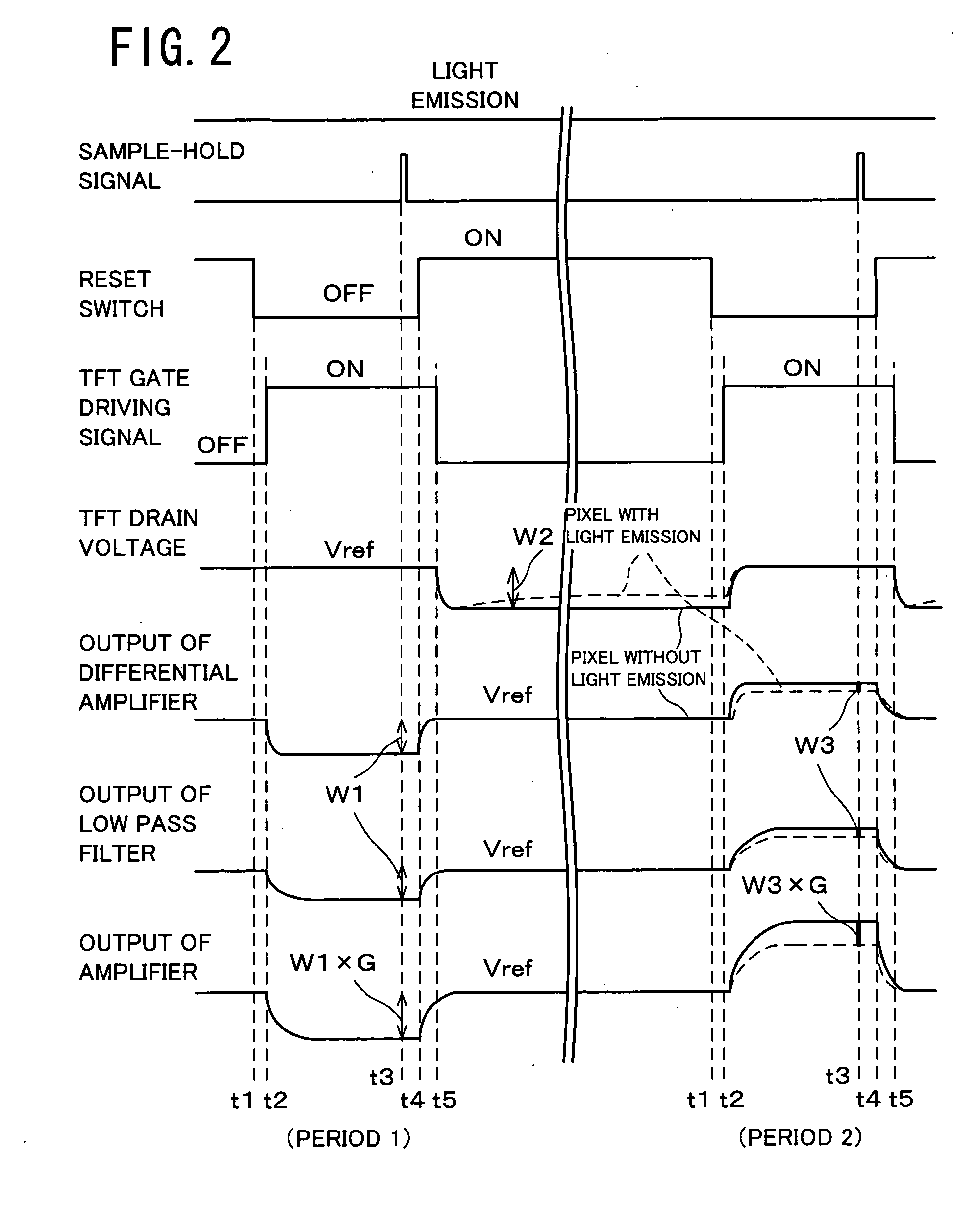
[0159] The structure and the operation of the photosensor in accordance with the present embodiment will be explained in reference to FIG. 7 and FIG. 8. FIG. 7 is block diagram schematically showing the structure corresponding to one pixel of another photoelectric converter in accordance with the present invention. FIG. 8 is a timing chart showing a detection operation in the photoelectric converter shown in FIG. 7.

[0160] As illustrated in FIG. 7, the photosensor in accordance with the present embodiment is characterized in that an electrode of the auxiliary capacitance on the opposite side of the TFT drain of the auxiliary...

third embodiment

[0179] A still another embodiment of the present invention will be explained. For convenience in explanations, members having the same functions as those of the second embodiment will be designated by the same reference numerals, and thus the descriptions thereof shall be omitted here. The same structures shown in FIG. 5 and FIG. 6 are adopted in the present embodiment.

[0180] The structure and the operation of the photosensor in accordance with the present embodiment will be explained in reference to FIG. 7 and FIG. 10. FIG. 10 is a timing chart showing a detection operation in the photoelectric converter shown in FIG. 7.

[0181] As illustrated in FIG. 7, the photosensor in accordance with the present embodiment is characterized in that an electrode of the auxiliary capacitance on the opposite side of the TFT drain of the auxiliary capacitance is driven by a voltage (CS electrode drive voltage 40) which is different from the reference voltage 23. Other than the foregoing, the struct...


PUM


Abstract

A sensor substrate (20) which includes phototransistors (7), each having a photosensitive semiconductor layer, and auxiliary capacitances (17) connected to the drain electrodes D of the corresponding phototransistors (7), and detecting ICs (25) for detecting a photoelectric conversion amount of the sensor substrate (20), which is connected to a source electrode S of the phototransistor (7), are provided. In the auxiliary capacitance (17), a predetermined amount of charge is stored, and also stored are the charge as generated by an emission of a light beam onto a photosensitive semiconductor layer in the non-conductive state of the phototransistor (7). Each detecting IC (25) detects a photoelectric conversion amount of the sensor substrate (20) based on the amount of charge remaining in the auxiliary capacitance (17).

Description

TECHNICAL FIELD [0001] The present invention relates to a photoelectric converter for detecting a photoelectric conversion amount as converted by a photoelectric conversion element, and more particularly relates to an image input device and a two-dimensional image sensor adopting such photoelectric converter, suited for personal computers, information terminal equipments, etc. BACKGROUND ART [0002] Conventionally, as means for inputting an image in a personal computer, a facsimile machine, etc., adopted is an image input device (an image scanner, for example) adopting a combination of a 1D image sensor and a mechanical scanner. For such image input device, a mechanical scanning is necessary to scan an image in a document either by moving the 1D image sensor relative to the document or moving the document relative to the 1D image sensor. A problem therefore arises in that the speed of reading images is lowered, or the apparatus cannot be reduced in size and weight as desired. [0003] ...

Claims


Application Information

Patent Timeline
Patent Type & Authority Applications(United States)
IPC IPC(8): H04N5/335H04N5/374H01L27/146H04N5/376H01L29/786
CPCH01L27/14679H04N3/155H04N5/32H04N25/76
Inventor UEHARA, KAZUHIRO
Owner SHARP KK
Why Eureka
Try Eureka