Photosensor and photosensor array
a photosensor and array technology, applied in the field of photosensors and photosensor arrays, can solve the problems of increasing the cost of the photosensor array, and achieve the effect of simplifying the pixel structur
- Summary
- Abstract
- Description
- Claims
- Application Information
AI Technical Summary
Benefits of technology
Problems solved by technology
Method used
Image

Examples
first embodiment
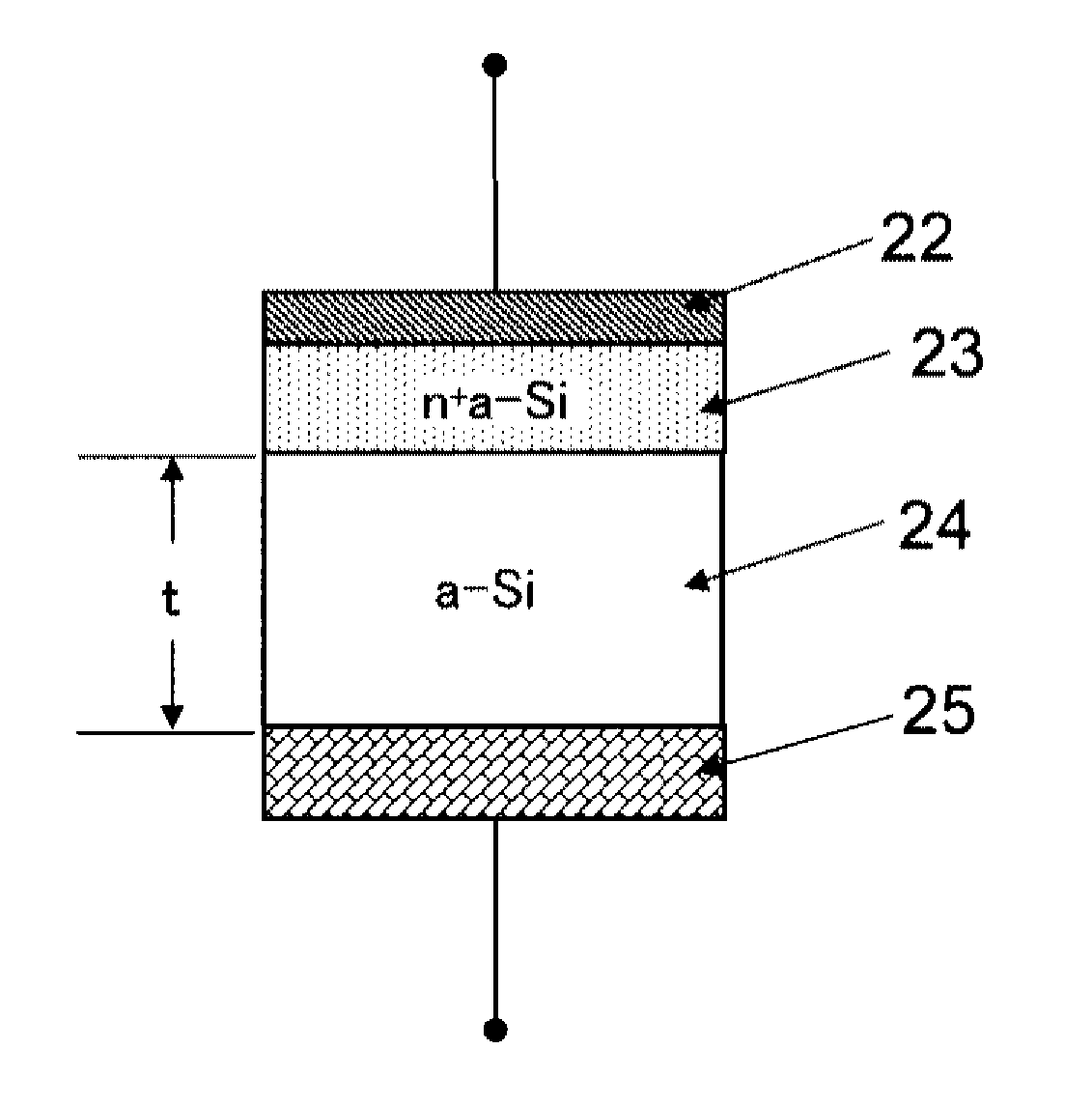
[0062]In the multiple embodiments of the present invention to be described below, an amorphous silicon film (a-Si) and an n-type amorphous silicon film (n+a-Si) doped with phosphorus are used as a photosensor element.
[0063]FIG. 1 is a cross-sectional view illustrating a cross-section structure of a photosensor for one pixel used in a photosensor array according to a first embodiment of the present invention. As illustrated in FIG. 1, a photosensor according to this embodiment includes a lower electrode 25, an amorphous silicon film (a-Si) 24 that is stacked on the lower electrode 25, an n-type amorphous silicon film (n+a-Si) 23 that is stacked on the amorphous silicon film (a-Si) 24 and doped with phosphorus, and an upper electrode 22 disposed on the n-type amorphous silicon film (n+a-Si) 23 doped with phosphorus.
[0064]That is, in this embodiment, the n-type amorphous silicon film (n+a-Si) 23 doped with phosphorus and the amorphous silicon film (a-Si) 24 are held between the upper e...
second embodiment
[0098]FIG. 9 is a circuit diagram illustrating a circuit configuration of a photosensor array according to a second embodiment. FIG. 10 is a timing chart illustrating a method of driving the photosensor array according to the second embodiment.
[0099]This embodiment is mainly different from the above-described first embodiment in that the photosensor pixels are reversely connected. In this case, the polarities of the drive voltage and the signal voltage are also reverse. That is, in the method of driving the photosensor array according to this embodiment, when, in the blanking period of one horizontal scanning period HSYNC, the signal RG becomes H level, and the reset transistors TLS turn on, the respective read lines S1, S2, are uniformly set to aground potential.
[0100]Hereinafter, the method of driving the photosensor array according to this embodiment will be described with reference to FIG. 10.
[0101]First, in the blanking period of one horizontal scanning period HSYNC, the signal...
third embodiment
[0110]In the photosensor arrays according to the above-described respective embodiments, a relatively large dark current component is always contained in the output signal voltage (or current). Also, because the dark current of amorphous silicon that is a high-resistant semiconductor has a temperature dependency, there is a need to correct the dark current component under the usage environment. The photosensor array according to this embodiment is configured to correct the dark current component.
[0111]FIG. 11 is a circuit diagram illustrating a circuit configuration of a photosensor array according to a third embodiment.
[0112]A difference between this embodiment and the first embodiment mainly resides in that a photosensor pixel PXD for dark current correction is disposed on each row of the photosensor array. The photosensor pixel PXD for dark current correction may be disposed in the photosensor array of the second embodiment.
[0113]In an example illustrated in FIG. 11, one photosen...
PUM
 Abstract
Description
Claims
Application Information
 - R&D
- Intellectual Property
- Life Sciences
- Materials
- Tech Scout
- Unparalleled Data Quality
- Higher Quality Content
- 60% Fewer Hallucinations
Browse by: Latest US Patents, China's latest patents, Technical Efficacy Thesaurus, Application Domain, Technology Topic, Popular Technical Reports.
© 2025 PatSnap. All rights reserved.Legal|Privacy policy|Modern Slavery Act Transparency Statement|Sitemap|About US| Contact US: help@patsnap.com