Pixel structure based on inkjet printing technology and method for manufacturing the same

a technology of inkjet printing and pixel structure, which is applied in the direction of solid-state devices, semiconductor devices, organic semiconductor devices, etc., can solve the problems that the ink-jet printer cannot meet the requirements for display panel manufacturing, the ink-jet printer cannot meet the requirements for manufacturing a higher-definition display product, and the process is complicated, so as to achieve the effect of improving the quality of the product and simple manufacturing of the pixel structur

Active Publication Date: 2019-09-05
SHENZHEN CHINA STAR OPTOELECTRONICS TECH CO LTD
View PDF0 Cites 1 Cited by
  • Summary
  • Abstract
  • Description
  • Claims
  • Application Information

AI Technical Summary

Benefits of technology

[0023]In the method for manufacturing the pixel structure based on ink-jet printing technology according to the present disclosure, the metal oxide semi-conductive material is used for forming the anode layer, and the anode layer is divided into conductive areas and semi-conductive areas by conductive treatment. The semi-conductive areas play a same role as the dielectric layer in the prior art. The method for manufacturing the pixel structure is simple because formation of the dielectric layer is not needed. Besides, an organic functional layer formed by ink jet has a uniform film thickness, which effectively improves quality of a product.

Problems solved by technology

The precision of an existing ink-jet printer cannot meet requirements for manufacture of the display panel gradually, and requirements for manufacture of a higher-definition display product cannot be met by the ink-jet printer due to its limitations.
Technical problems exist in such a process.
Therefore, the process is complicated.

Method used


Image

  • Pixel structure based on inkjet printing technology and method for manufacturing the same
  • Pixel structure based on inkjet printing technology and method for manufacturing the same
  • Pixel structure based on inkjet printing technology and method for manufacturing the same

Examples


Embodiment Construction

[0035]The present disclosure will be illustrated hereinafter with reference to the drawings.

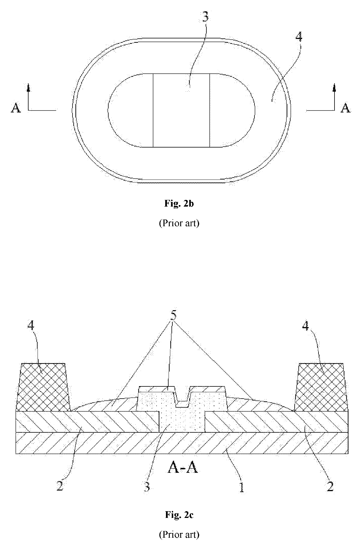
[0036]FIG. 3 is a flow chart of a method for manufacturing a pixel structure based on ink-jet printing technology in the present embodiment. It can be seen from FIG. 3 that, the method comprises following steps.

[0037]In step S1: an anode layer is formed on a substrate using a metal oxide semi-conductive material, and the anode layer is patterned.

[0038]In step S2: a photoresist layer is formed on the anode layer, and the photoresist layer is patterned. The patterned photoresist layer covers the anode layer partially.

[0039]In step S3: conductive treatment is performed to portions of the anode layer which are not covered by the photoresist layer, and then the photoresist layer is removed.

[0040]In step S4: a pixel defining layer is formed on the anode layer, and a plurality of through-holes, which are spaced from one another, are formed on the pixel defining layer. The anode layer at the through-...


PUM

PropertyMeasurementUnit
semi-conductiveaaaaaaaaaa
areaaaaaaaaaaa
structureaaaaaaaaaa

Abstract

Disclosed are a pixel structure based on ink-jet printing technology and a method for manufacturing the same. In the pixel structure and in the method for manufacturing the same, a metal oxide semi-conductive material is used for forming an anode layer. The anode layer is divided into conductive areas and semi-conductive areas by conductive treatment. The semi-conductive areas play a same role as a dielectric layer in the prior art. The method for manufacturing the pixel structure is simple because formation of the dielectric layer is not needed. An organic functional layer formed by ink-jet has a uniform film thickness, which effectively improves quality of a product.

Description

CROSS-REFERENCE TO RELATED APPLICATIONS[0001]This application claims the priority of Chinese patent application CN 201710464655.8, entitled “Pixel structure based on inkjet printing technology and method for manufacturing the same” and filed on Jun. 19, 2017, the entirety of which is incorporated herein by reference.FIELD OF THE INVENTION[0002]The present disclosure relates to the field of OLED (organic light-emitting diode) manufacturing, and in particular, to a pixel structure based on inkjet printing technology and a method for manufacturing the same.BACKGROUND OF THE INVENTION[0003]An organic light-emitting diode (OLED) display device, which is also known as an organic electroluminescent display device, has many advantages. For example, the OLED display device is self-luminous, can be driven at a low voltage. Moreover, the OLED display device has high luminous efficiency, short response time, high definition and contrast, a wide viewing angle, and a wide working temperature rang...

Claims


Application Information

Patent Timeline
Patent Type & Authority Applications(United States)
IPC IPC(8): H01L51/00H01L27/32H01L51/50H01L51/52
CPCH01L51/0005H01L27/3246H01L51/0023H01L51/5012H01L51/5056H01L2227/323H01L51/5088H01L51/5092H01L51/5209H01L51/5221H01L2251/308H01L51/5072H10K71/135H10K50/81H10K71/00H10K59/353H10K59/122H10K71/60H10K50/11H10K50/15H10K50/16H10K50/17H10K50/82H10K50/171H10K50/813H10K71/621H10K59/1201H10K2102/103
Inventor FANG, CHUN HSIANGWU, YUAN CHUNLU, PO YEN
Owner SHENZHEN CHINA STAR OPTOELECTRONICS TECH CO LTD
Why Eureka
Try Eureka