Organic light emitting display device

a light-emitting display and organic technology, applied in semiconductor devices, instruments, electrical devices, etc., can solve problems such as image sticking phenomenon, and achieve the effects of high resolution, simplified pixel structure, and increased design margin

Active Publication Date: 2020-05-14
LG DISPLAY CO LTD
View PDF0 Cites 3 Cited by
  • Summary
  • Abstract
  • Description
  • Claims
  • Application Information

AI Technical Summary

Benefits of technology

[0010]Since the organic light emitting diode display device according to the present disclosure does not require additional patterns and switch elements and performs a sensing operation using only the configuration of an internal compensation circuit necessary during a displaying period, the pixel structure can be simplified.
[0011]Since a sensing voltage is obtained by using a data line, an initialization line can be disposed as a horizontal line. As a result, the design margin can be increased, which is advantageous in realizing a high resolution.

Problems solved by technology

The difference in the deterioration of the OLEDs between the pixels can cause a luminance variation and can result in image sticking phenomenon.

Method used


Image

  • Organic light emitting display device
  • Organic light emitting display device
  • Organic light emitting display device

Examples


first embodiment

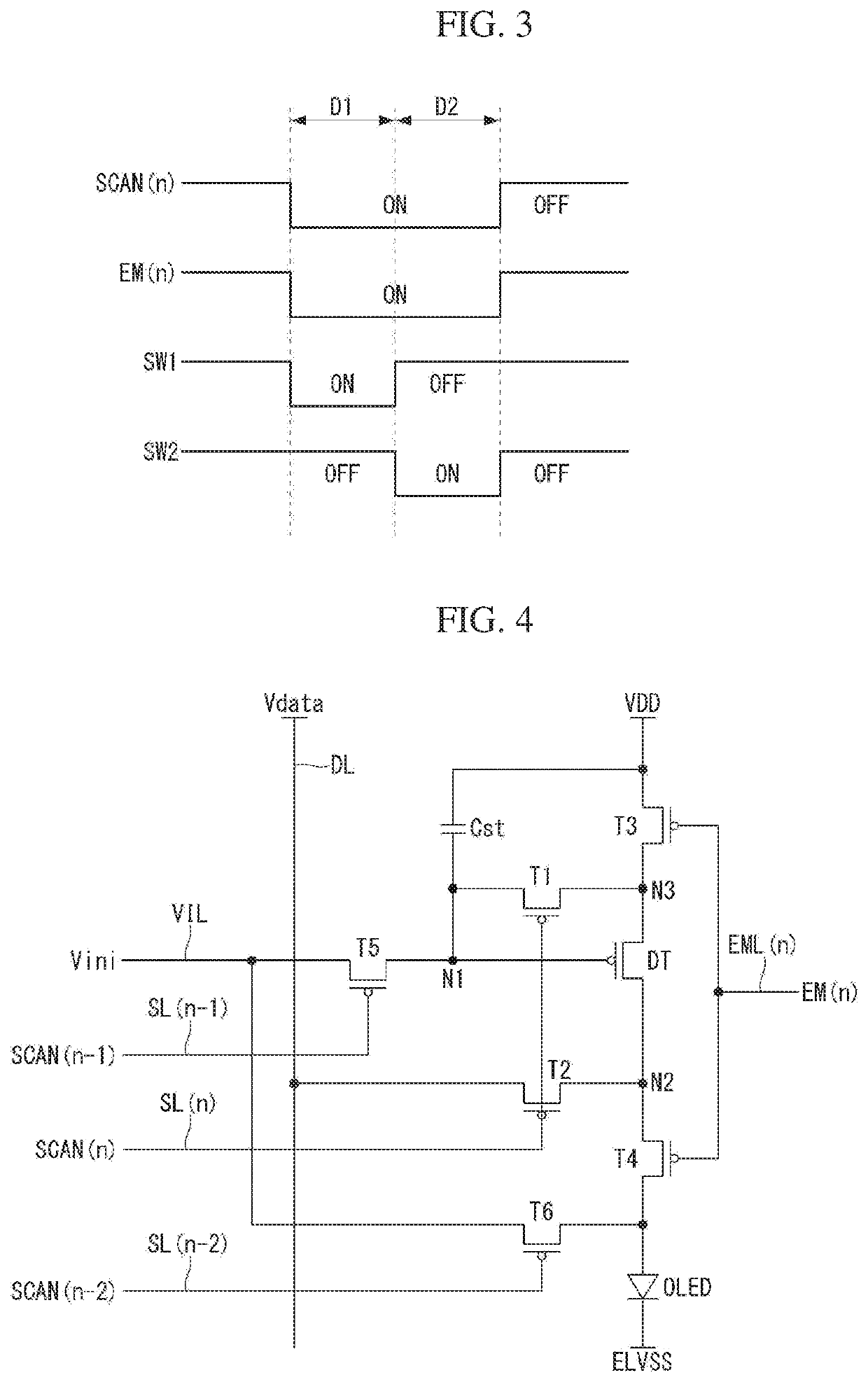
[0041]FIG. 4 is a diagram showing a pixel circuit according to the present disclosure.

[0042]Referring to FIG. 4, the pixel (e.g., P in FIG. 1) according to the first embodiment includes an OLED, a driving transistor DT, a first transistor T1, a scan transistor T2, first and second emission control transistors T4 and T3, first and second initialization transistors T5 and T6 and a storage capacitor Cst.

[0043]The driving transistor DT controls the driving current applied to the OLED according to its source-gate voltage Vsg. In the driving transistor DT, a gate electrode is connected to a first node N1, a drain electrode is connected to a second node N2, and a source electrode is connected to the input terminal of a high potential voltage VDD through the second emission control transistor T3.

[0044]The first transistor T1 includes a gate electrode connected to an n-th scan line SL(n), a source electrode connected to a third node N3, and a drain electrode connected to the first node N1. T...

second embodiment

[0093]The pixel circuit compensates the change of the threshold voltage of the driving transistor DT in real time within the displaying period according to the internal compensation scheme.

[0094]FIG. 10 is a diagram illustrating the timings of gate signals in the displaying period according to the second embodiment, and FIGS. 11A to 11D are equivalent circuit diagrams of pixels in a first initialization period, a second initialization period, a sampling period, and a light emission period, respectively. Hereinafter, in the second embodiment, the same reference numerals and names are used for components substantially the same as those in the first embodiment described above.

[0095]Referring to FIGS. 8 to 11D, the operations of the pixel are as follows which emits light while compensating for the threshold voltage change of the driving transistor in real time.

[0096]Referring to FIGS. 8 to 10 and 11A, in the first initialization period Ti1, the (n-2)-th scan signal SCAN(n-2) maintains ...


PUM

PropertyMeasurementUnit
voltageaaaaaaaaaa
anode voltageaaaaaaaaaa
turn-on voltageaaaaaaaaaa

Abstract

An organic light emitting display device can include an organic light emitting diode (OLED), a driving transistor connected to an anode electrode of the OLED, a scan transistor, a digital-to-analog converter (DAC) and a sensing unit. The scan transistor is connected the anode electrode of the OLED and a data line. The DAC supplies a data voltage for displaying to the data line in a displaying period and supplies a data voltage for sensing to the data line in a sensing period. The sensing unit obtains an anode voltage of the OLED as a sensing voltage through the data line in the sensing period.

Description

[0001]This application claims the priority benefit of Korean Patent Application No. 10-2018-0138090 filed on Nov. 12, 2018 in the Republic of Korea, which is incorporated herein by reference for all purposes as if fully set forth herein.BACKGROUNDField[0002]The present disclosure relates to an organic light emitting display device of an active matrix type.Discussion of the Related Art[0003]The organic light emitting display device of an active matrix type includes an organic light emitting diode (OLED) emitting light itself, and is advantageous in that response speed, luminous efficiency and luminance are high, and viewing angle is large.[0004]The OLED which is a self light-emitting element includes anode and cathode electrodes and an organic compound layer formed therebetween. The organic compound layer comprises a hole injection layer, a hole transport layer, an emission layer, an electron transport layer, and an electron injection layer. When driving voltages are applied to the a...

Claims


Application Information

Patent Timeline
Patent Type & Authority Applications(United States)
IPC IPC(8): G09G3/3258G09G3/3233G09G3/3275H01L27/32
CPCH01L27/3248G09G2320/045G09G2320/0233G09G3/3275G09G2300/0426H01L27/124G09G3/3233G09G3/3258G09G2310/027H01L27/3276G09G2300/0809G09G3/3225G09G2320/0295G09G2300/0819G09G2300/0842G09G2300/0861G09G2320/0238G09G2310/0256G09G2300/0439G09G2320/043G09G2320/048H10K59/123H10K59/131
Inventor HONG, SOONHWANLEE, CHEOLHWAN
Owner LG DISPLAY CO LTD
Why Eureka
Try Eureka