
Method for fabricating self-aligned nanostructure using self-assembly block copolymers, and structures fabricated therefrom

a technology of self-assembly block and nanostructure, which is applied in the field of fabrication of self-aligned nanostructures, can solve the problems of harsh reactive ion etching process on metallic lines

Active Publication Date: 2009-09-17
GLOBALFOUNDRIES US INC
View PDF3 Cites 83 Cited by
  • Summary
  • Abstract
  • Description
  • Claims
  • Application Information

AI Technical Summary

Benefits of technology

[0033]wherein Lo is a natural periodicity for block copolymer phase separation and ranges from about 40 nm to about 120 nm. It is noted that smaller periodicities have been contemplated, so long as the periodicity is not too small to permit separation of the diblock, in accordance with the present invention.

Problems solved by technology

One disadvantage to this prior art approach is the exposure of the metallic lines to a harsh reactive ion etch process that is required for patterning of the interlevel dielectric material.

Method used


Image

  • Method for fabricating self-aligned nanostructure using self-assembly block copolymers, and structures fabricated therefrom
  • Method for fabricating self-aligned nanostructure using self-assembly block copolymers, and structures fabricated therefrom
  • Method for fabricating self-aligned nanostructure using self-assembly block copolymers, and structures fabricated therefrom

Examples


Embodiment Construction

[0040]Detailed embodiments of the present invention are disclosed herein; however, it is to be understood that the disclosed embodiments are merely illustrative of the invention that may be embodied in various forms. In addition, each of the examples given in connection with the various embodiments of the invention are intended to be illustrative, and not restrictive. Further, the figures are not necessarily to scale, some features may be exaggerated to show details of particular components. Therefore, specific structural and functional details disclosed herein are not to be interpreted as limiting, but merely as a representative basis for teaching one skilled in the art to variously employ the present invention.

[0041]The embodiments of the present invention relate to novel patterning methods and related structures for microelectronic devices. When describing the inventive structures and methods, the following terms have the following meanings, unless otherwise indicated.

[0042]As us...


PUM

PropertyMeasurementUnit
widthaaaaaaaaaa
widthaaaaaaaaaa
thicknessaaaaaaaaaa

Abstract

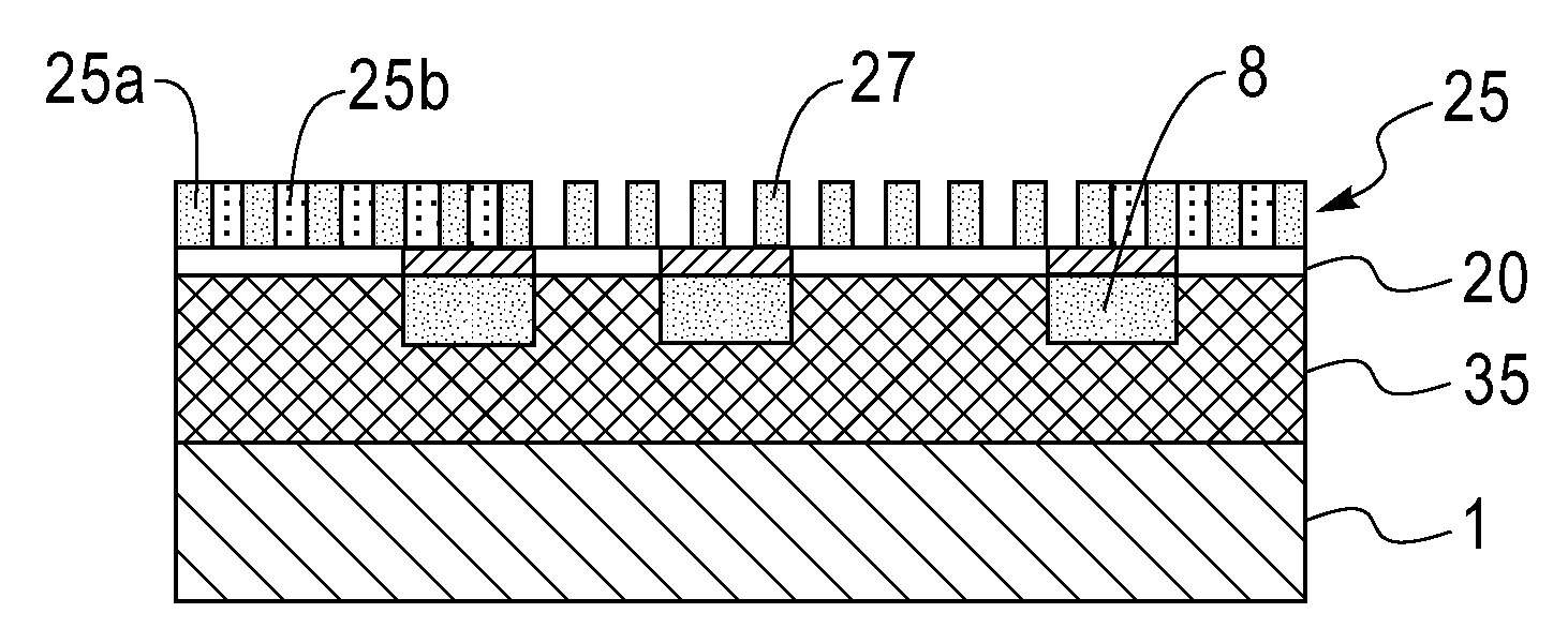
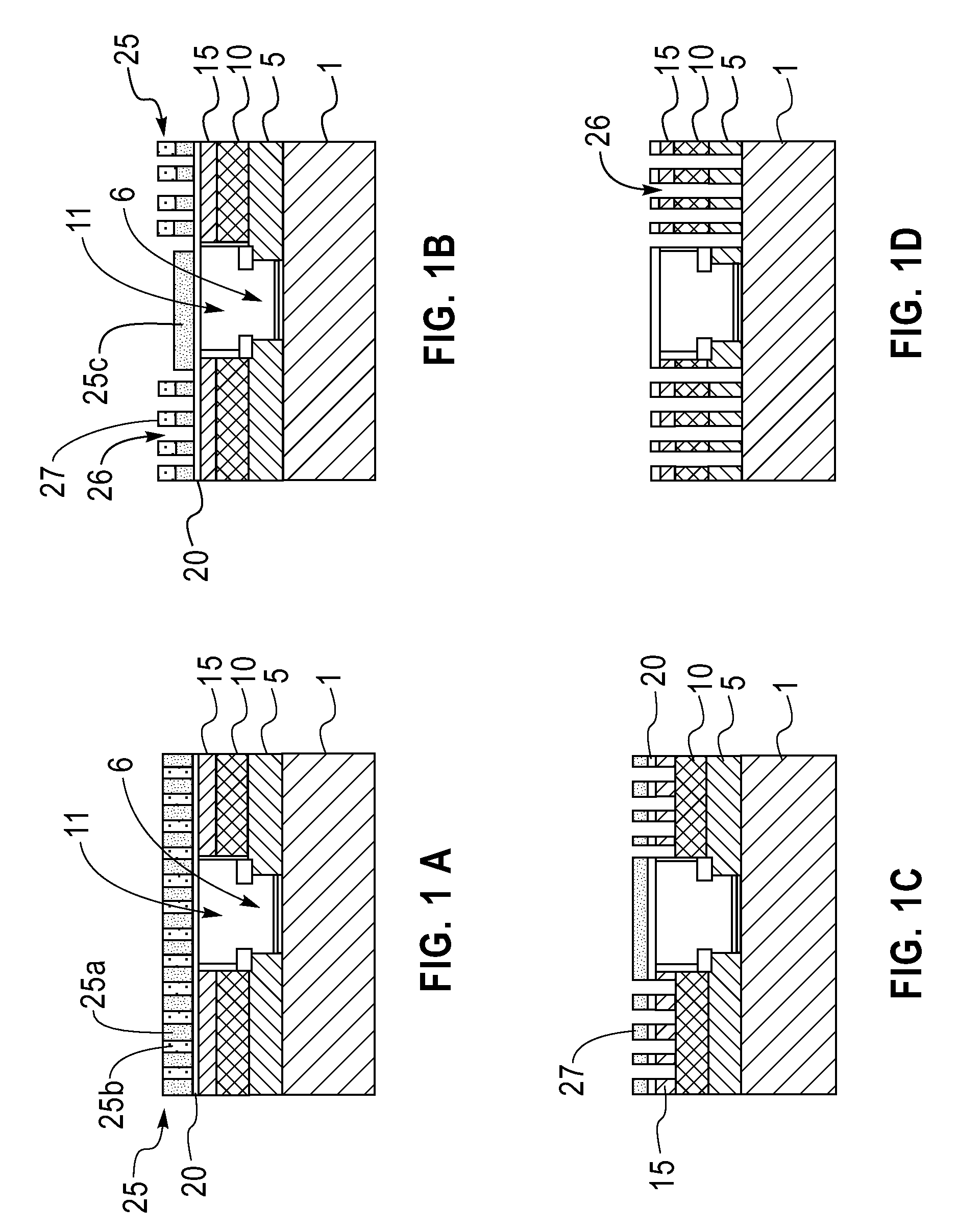
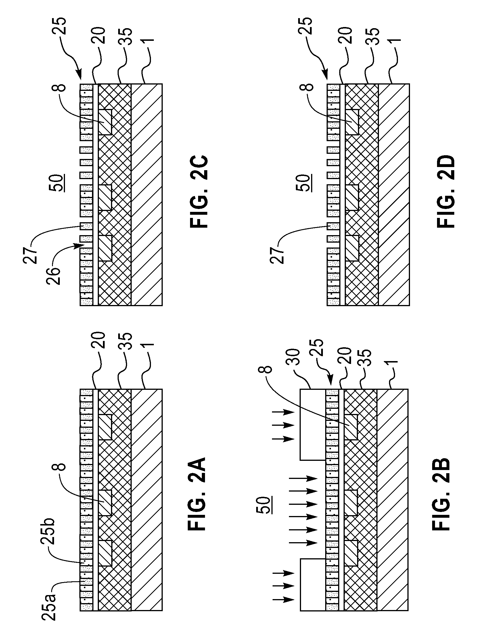
In one embodiment, the present invention provides a method for patterning a surface that includes forming a block copolymer atop a heterogeneous reflectivity surface, wherein the block copolymer is segregated into first and second units; applying a radiation to the first units and second units, wherein the heterogeneous reflectivity surface produces an exposed portion of the first units and the second units; and applying a development cycle to selectively remove at least one of the exposed first and second units of the segregated copolymer film to provide a pattern.

Description

FIELD OF THE INVENTION [0001]The present invention relates to the fabrication of self-aligned nanostructures, and more specifically to nanostructures generated using a combination of self-assembly and self-aligned imaging provided by copolymer films.BACKGROUND OF THE INVENTION [0002]The fabrication of Very-Large Scale Integrated (VLSI) or Ultra-Large Scale Integrated circuit (ULSI) requires metallic wiring that connects individual devices in a semiconductor chip, to one another. One method of creating this wiring network on such small scale is a dual damascene (DD) process. In a typical DD process, an interlayer dielectric (ILD) typically comprising two dielectric layers (e.g., a via level dielectric and a line level dielectric) is formed on a substrate. In general, the via and line level dielectrics can be made of the same or different insulating films and in the former case applied as a single monolithic layer. A hard mask layer is optionally employed to facilitate etch selectivit...

Claims


Application Information

Patent Timeline
Patent Type & Authority Applications(United States)
IPC IPC(8): G03F7/00
CPCB82Y10/00G03F7/039G03F7/0002B82Y40/00
Inventor BLACK, CHARLES T.COLBURN, MATTHEW E.RATH, DAVID L.
Owner GLOBALFOUNDRIES US INC
Features
  • Generate Ideas
  • Intellectual Property
  • Life Sciences
  • Materials
  • Tech Scout
  • Unparalleled Data Quality
  • Higher Quality Content
  • 60% Fewer Hallucinations
Learn More