

Touch Panel Device
a technology device body, which is applied in the field of touch panel devices, can solve the problems of reducing the yield rate of capacitive touch panel devices and interfering with detection, and achieve the effect of simple structure and easy manufacturing
- Summary
- Abstract
- Description
- Claims
- Application Information
AI Technical Summary
Benefits of technology
Problems solved by technology
Method used
Image

Examples
first embodiment
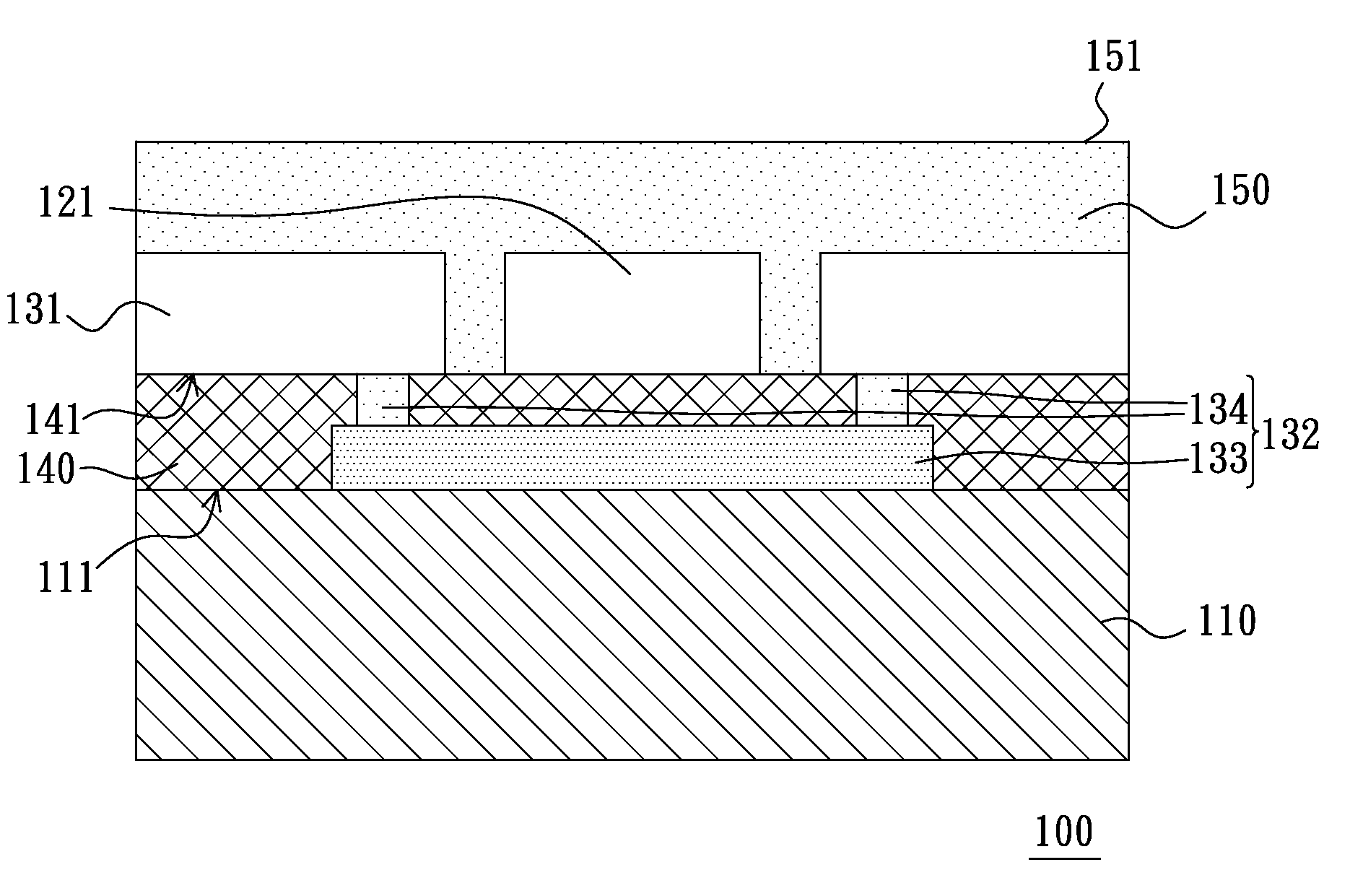
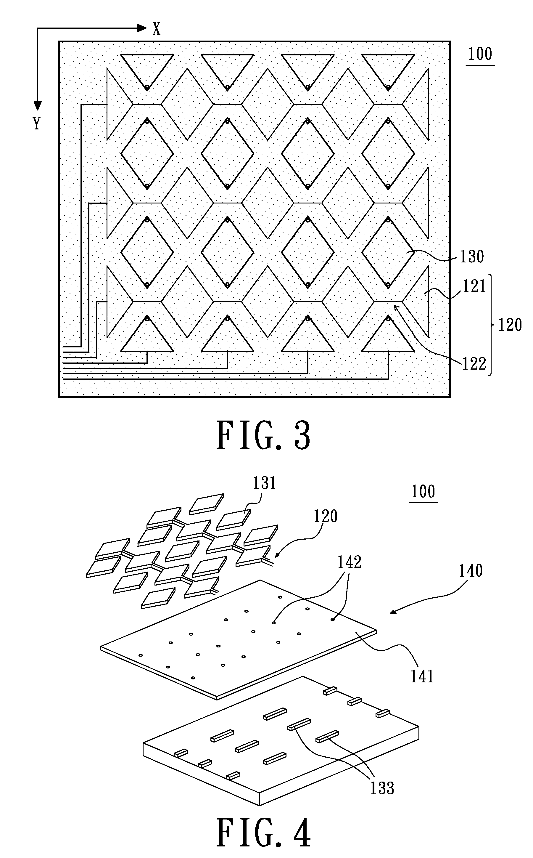
[0031]Referring to FIG. 2 and FIG. 3, a touch panel device according to the present invention is shown. The touch panel device 100 includes a substrate 110, at least one first electrode group 120, at least one second electrode group 130, an insulating layer 140, and an anti-scratch layer 150.
[0032]In this embodiment, the touch panel device 100 includes a plurality of first electrode groups 120 and a plurality of second electrode groups 130. The first electrode groups 120 and the second electrode groups 130 are disposed at a same side of the substrate 110. The insulating layer 140 is formed on a surface of the substrate 110. The anti-scratch layer 150 covers the first electrode groups 120 and the second electrode groups 130 for protecting them. In addition, an anti-reflection layer or other protecting layer can be formed on the anti-reflection layer 150.
[0033]Each of the first electrode groups 120 includes a plurality of first electrodes 121 and a plurality of first connecting lines ...
second embodiment
[0045]Referring to FIG. 5 to FIG. 8, a touch panel device 200 according to the present invention is shown. The touch panel device 200 is similar to the touch panel device 100 except for the configurations of second electrode groups 230. The touch panel device 200 includes a plurality of second electrode groups 230. Each second electrode group 230 includes a plurality of second electrodes 231 and a bridge connecting wire 232 for electrically connecting two adjacent second electrodes 231. The bridge connecting wire 232 includes a first conductive part 233 and a plurality of second conductive parts 234 electrically connected to the first conductive part 233. The first conductive part 233 is a line-shaped conducting line corresponding to the plurality of second electrodes 231. The number of the second conductive parts 234 is equal to the number of the second electrodes 231 such that the second conductive parts 234 respectively correspond to the second electrodes 231. Each second electro...
third embodiment
[0046]Understandably, the position of connections between the second conductive parts 234 and the second electrodes 231 are not limited to the end of the second electrodes 231. In an alternative embodiment of the present invention, the second conductive parts 234 can be electrically connected to any portion of the second electrodes 231. For example, referring to FIG. 9 to FIG. 10, a touch panel device 300 according to the present invention is similar to the touch panel device 200. A difference therebetween is that an end of each second conductive part 334 is connected to the first conductive part 233 and the other end of each second conductive part 334 is connected to a middle portion of the second electrodes 231.
[0047]Comparing with the conventional touch panel device, the touch panel devices 200, 300 have advantages same with that of the touch panel device 100. Furthermore, because the touch panel devices 200, 300 only have one line-shaped first conductive part 233, 333 respective...
PUM
 Abstract
Description
Claims
Application Information