Non-contact type IC card

a non-contact type, ic chip technology, applied in the direction of unauthorized memory use protection, instruments, printing, etc., can solve the problems of achieve the effect of preventing the electrostatic discharge failure of the ic chip

Inactive Publication Date: 2009-10-08
KYODO INSATU KK KYODO PRINTING CO LTD
View PDF12 Cites 53 Cited by
  • Summary
  • Abstract
  • Description
  • Claims
  • Application Information

AI Technical Summary

Benefits of technology

[0024]Even when an electrostatic test prescribed by “JIS X 6305-6:2001 (ISO/IEC 10373-6:2001)” or “JIS X 6305-7:2001 (ISO/IEC 10373-7:2001)” is performed and static electricity is discharged to the metal reflective layer, the non-contact type IC card

Problems solved by technology

Finally, the discharge current flows into an IC chip connected to the

Method used


Image

  • Non-contact type IC card
  • Non-contact type IC card
  • Non-contact type IC card

Examples


first exemplary embodiment

Structure of Non-Contact Type IC Card

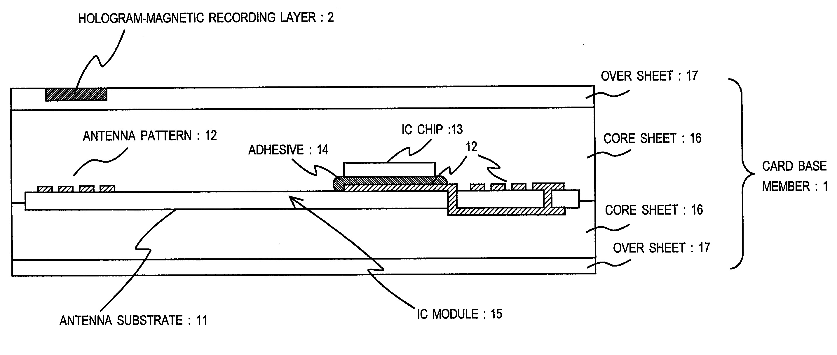
[0030]First, the structure of a non-contact type IC card according to this exemplary embodiment will be described with reference to FIG. 1.

[0031]As shown in FIG. 1, the non-contact type IC card according to this exemplary embodiment includes a card base member 1 and a hologram-magnetic recording layer 2. Further, an antenna 12 and an IC chip 13 are embedded in the card base member 1 of this exemplary embodiment as shown in FIG. 1. The IC chip 13 is connected to the antenna 12, and embedded in the card base member 1.

Structure of Card Base Member 1

[0032]The structure of the card base member 1 of the non-contact type IC card according to this exemplary embodiment will be described below with reference to FIG. 1.

[0033]The card base member 1 of the non-contact type IC card according to this exemplary embodiment is structured as follows: As shown in FIG. 1, antenna pattern 12, such as helicoidal antennas or capacitors, form an antenna pattern on an an...

second exemplary embodiment

[0080]A non-contact type IC card according to a second exemplary embodiment will be described below.

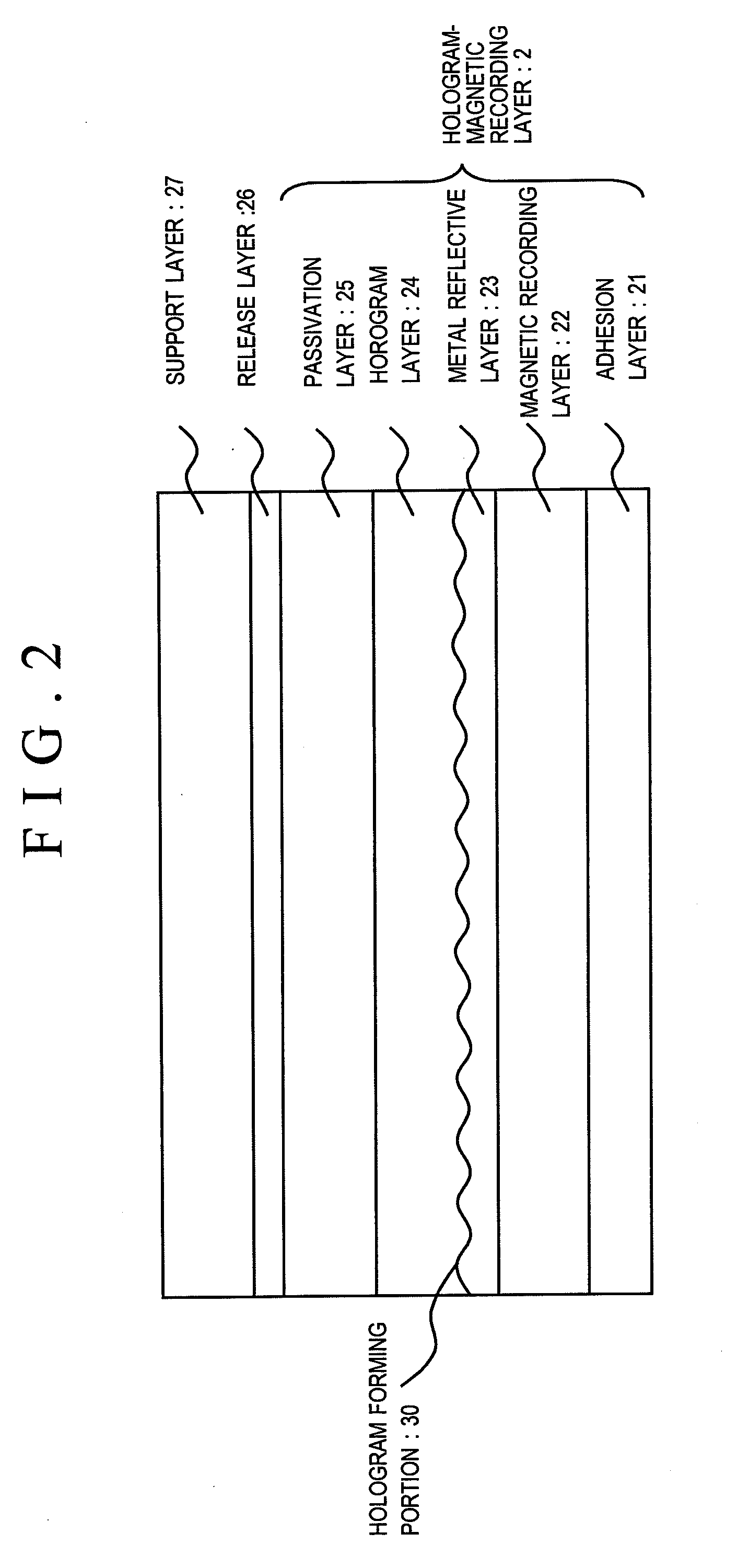
[0081]A non-contact type IC card according to a second exemplary embodiment is characterized in that a metal reflective layer 23 of a hologram-magnetic recording layer 2 is formed to have a surface resistivity of 7.02 (Ω / □) or more. Accordingly, even when an electrostatic test prescribed by “JIS X 6305-6:2001 (ISO / IEC 10373-6:2001)” or “JIS X 6305-7:2001 (ISO / IEC 10373-7:2001)” is performed and static electricity is discharged to the metal reflective layer 23, it is possible to limit discharge current that flows from the metal reflective layer 23 to an antenna 12. As a result, it is possible to prevent electrostatic discharge failure of an IC chip 13 embedded in the IC card. The non-contact type IC card according to the second exemplary embodiment will be described below with reference to FIGS. 8 and 9.

[0082]The non-contact type IC card according to the second exemplary embodiment inc...


PUM


Abstract

There is provided a non-contact type IC card that prevents electrostatic discharge failure of an IC chip embedded in an IC card.
A non-contact type IC card includes at least a magnetic recording layer, a metal reflective layer, and a hologram layer, which are sequentially laminated on a card base member, and an antenna and an IC chip connected to the antenna that are embedded in the card base member. The metal reflective layer is made of a material of which electric conductivity is smaller than 28.9×10⁶/Ωm, or is composed of a thin film of which surface resistivity is 7.02 (Ω/□) or more.

Description

TECHNICAL FIELD[0001]The present invention relates to a non-contact type IC card, and more particularly, to a non-contact type IC card including a magnetic recording layer, a metal reflective layer, and a hologram layer that are provided on at least one surface of a card base member, and an IC chip and a communication antenna that are embedded in the card base member, thereby being capable of transmitting and receiving data in a non-contact manner.BACKGROUND ART[0002]As a card technology has been developed in recent years, there are IC cards, which can be used for various purposes, as an information recording medium used in various communication systems. The IC cards are classified into a contact type IC card that can write and read information by coming in contact with a dedicated device, and a non-contact type IC card that can write and read information only by approaching a dedicated device.[0003]Since these IC cards have higher security and a large amount of information capable ...

Claims


Application Information

Patent Timeline
IPC IPC(8): G06K19/06G06K19/02
CPCG06K19/07735G06K19/16G06K19/083G06K19/07749B42D25/305B42D25/328G06K19/07G06K19/077
Inventor FUJITA, MINORUOSAWA, HARUHIKOTSUSHIO, HAJIMENAGUMO, AKIKO
Owner KYODO INSATU KK KYODO PRINTING CO LTD
Why Eureka
Try Eureka