METHOD FOR FABRICATION OF SEMIPOLAR (Al, In, Ga, B)N BASED LIGHT EMITTING DIODES

a light-emitting diode and semi-polar technology, applied in the field of yellow light-emitting diodes, can solve the problems of red-shifted emission, restricted carrier recombination efficiency, and undesirable quantum-confined stark effect of c-plane quantum well (qw) structures in iii-nitride-based optoelectronic and electronic devices,

Active Publication Date: 2009-10-08
RGT UNIV OF CALIFORNIA
View PDF3 Cites 555 Cited by
  • Summary
  • Abstract
  • Description
  • Claims
  • Application Information

AI Technical Summary

Benefits of technology

[0019]The present invention further discloses a white LED device comprised of a blue light emitting QW and a yellow light emitting QW grown on one or more III-nitride based semipolar planes. Typically, the white LED device comprises MQWs that are comprised of the blue-light emitting QW that is a first InGaN QW, with a first In composition for emitting blue light, and the yellow-light emitting QW that is a second InGaN QW, with a second In composition for emitting yellow light.
[0020]The present invention further discloses a method of fabricating the yellow, amber, or red LED, by growth on at least one III-nitride based semipolar plane, so that the LED emits light with a peak emission wavelength

Problems solved by technology

However, conventional c-plane quantum well (QW) structures in III-nitride based optoelectronic and electronic devices suffer from the undesirable quantum-confined Stark effect (QCSE), due to the existence of strong piezoelectric and spontaneous polarizations.
The strong built-in electric fields along the c-direction cause spatial separation of electrons and holes that in turn give rise to restricted carrier recombination efficiency, reduced oscillator strength, and red-

Method used


Image

  • METHOD FOR FABRICATION OF SEMIPOLAR (Al, In, Ga, B)N BASED LIGHT EMITTING DIODES
  • METHOD FOR FABRICATION OF SEMIPOLAR (Al, In, Ga, B)N BASED LIGHT EMITTING DIODES
  • METHOD FOR FABRICATION OF SEMIPOLAR (Al, In, Ga, B)N BASED LIGHT EMITTING DIODES

Examples


Embodiment Construction

[0034]In the following description of the preferred embodiment, reference is made to the accompanying drawings which form a part hereof, and in which is shown by way of illustration a specific embodiment in which the invention may be practiced. It is to be understood that other embodiments may be utilized and structural changes may be made without departing from the scope of the present invention.

[0035]Overview

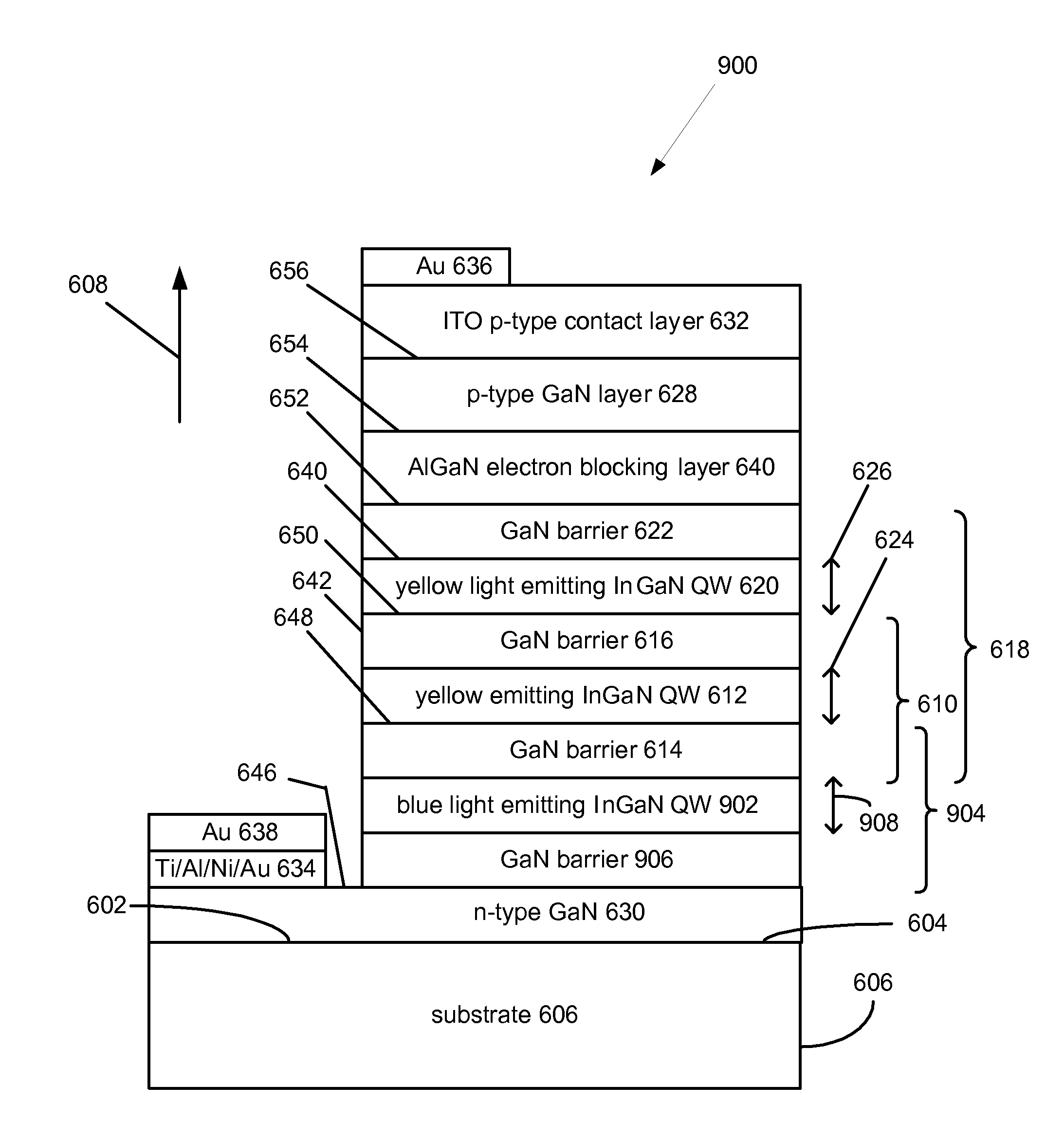
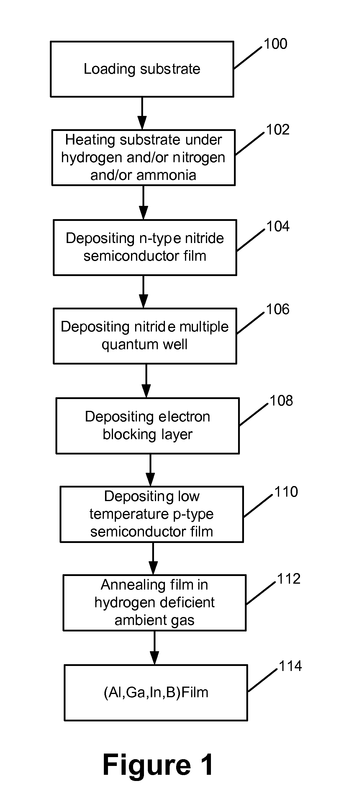
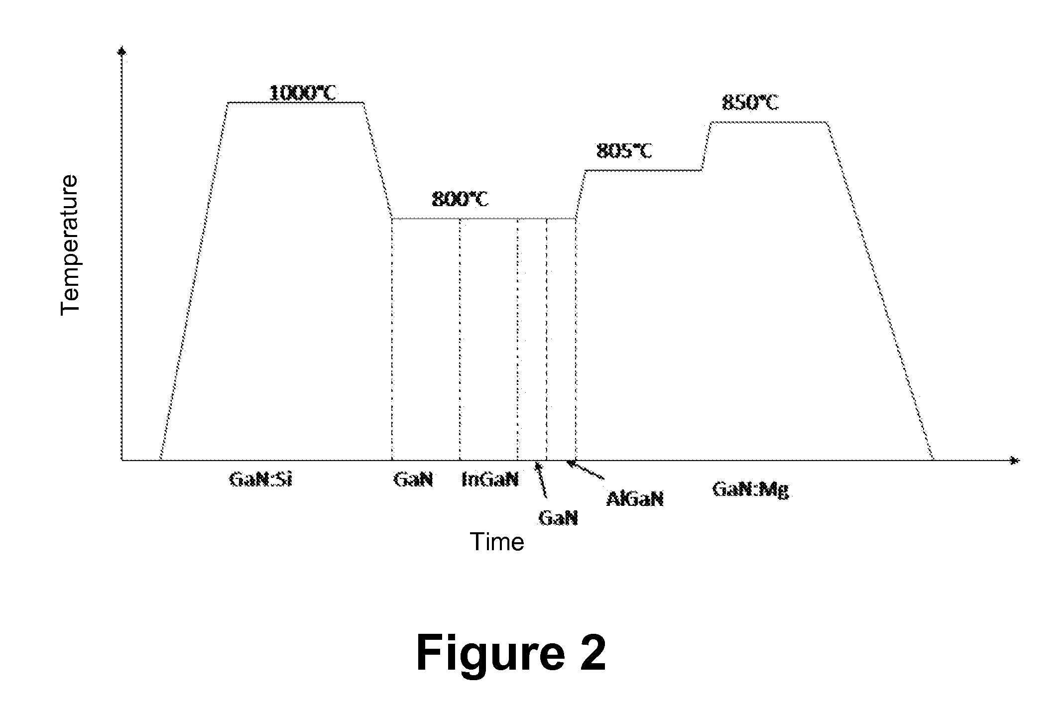
[0036]The present invention describes a method for fabrication of blue, green, yellow, white, and other color LEDs with a bulk semipolar GaN substrate such as {10-1-1}, {11-22}, and other planes. Semipolar (Al, In, Ga, B)N semiconductor crystals allow the fabrication of a multilayer structure with zero, or reduced, internal electric fields resulting from internal polarization discontinuities within the structure, as described in previous disclosures. This invention describes the first yellow LEDs in III-nitride based optoelectronics. Further, the invention incorporates a low t...


PUM


Abstract

A yellow Light Emitting Diode (LED) with a peak emission wavelength in the range 560-580 nm is disclosed. The LED is grown on one or more III-nitride-based semipolar planes and an active layer of the LED is composed of indium (In) containing single or multi-quantum well structures. The LED quantum wells have a thickness in the range 2-7 nm. A multi-color LED or white LED comprised of at least one semipolar yellow LED is also disclosed.

Description

CROSS REFERENCE TO RELATED APPLICATIONS[0001]This application claims the benefit under 35 U.S.C. Section 119(e) of co-pending and commonly-assigned U.S. Provisional Patent Application Ser. No. 61 / 042,644, filed on Apr. 4, 2008, by Hitoshi Sato, Hirohiko Hirasawa, Roy B. Chung, Steven P. DenBaars, James S. Speck and Shuji Nakamura, entitled “METHOD FOR FABRICATION OF SEMIPOLAR (Al,In,Ga,B)N BASED LIGHT EMITTING DIODES,” attorneys' docket number 30794.264-US-P1 (2008-415-1), which application is incorporated by reference herein.[0002]This application is related to the following co-pending and commonly-assigned applications:[0003]U.S. Utility patent application Ser. No. ______, filed on same date herewith, by Hitoshi Sato, Roy B. Chung, Feng Wu, James S. Speck, Steven P. DenBaars and Shuji Nakamura, entitled “MOCVD GROWTH TECHNIQUE FOR PLANAR SEMIPOLAR (Al, In, Ga, B)N BASED LIGHT EMITTING DIODES,” attorney's docket number 30794.274-US-U1 (2008-534), which application claims the benefi...

Claims


Application Information

Patent Timeline
IPC IPC(8): H01L33/00H01L21/02H01L33/02H01L33/32
CPCH01L21/0254H01L21/02579H01L21/02609Y10S977/755H01L33/02H01L33/32H01L33/08H01L21/0262
Inventor SATO, HITOSHIHIRASAWA, HIROHIKOCHUNG, ROY B.DENBAARS, STEVEN P.SPECK, JAMES S.NAKAMURA, SHUJI
Owner RGT UNIV OF CALIFORNIA
Why Eureka
Try Eureka