Display substrate and method of manufacturing the same

a technology of display substrate and substrate, which is applied in the field of display substrate, can solve the problems of deteriorating the display quality of the lcd device, and achieve the effects of reducing the resistance of metal wiring and enhancing the aperture ratio

Active Publication Date: 2009-10-08
SAMSUNG DISPLAY CO LTD
View PDF7 Cites 2 Cited by
  • Summary
  • Abstract
  • Description
  • Claims
  • Application Information

AI Technical Summary

Benefits of technology

[0012]According to a display substrate and a method of manufacturing the display substrate, a metal wiring is formed in a trench defined by color filters, so that the resistance of the metal wiring may be decreased and an aperture ratio may be enhanced.

Problems solved by technology

A misalignment, which may be generated when the TFT substrate and the color filter substrate are coupled with each other, may deteriorate the display quality of the LCD device.

Method used


Image

  • Display substrate and method of manufacturing the same
  • Display substrate and method of manufacturing the same
  • Display substrate and method of manufacturing the same

Examples


example embodiment 1

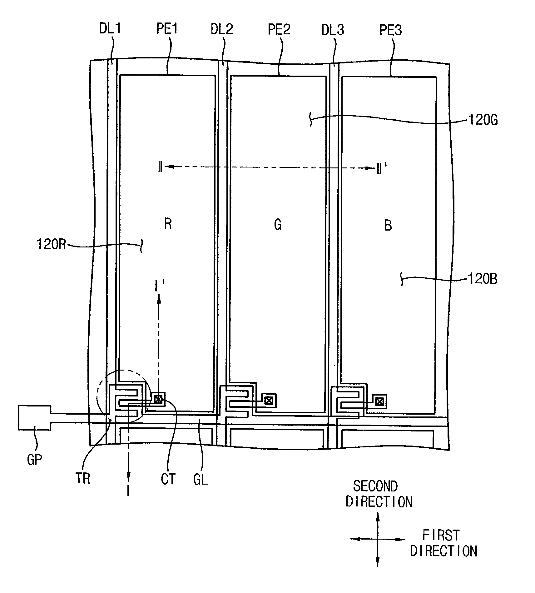
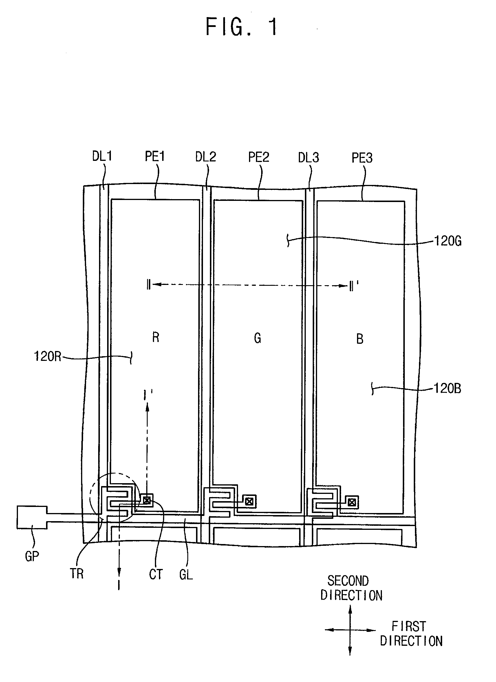
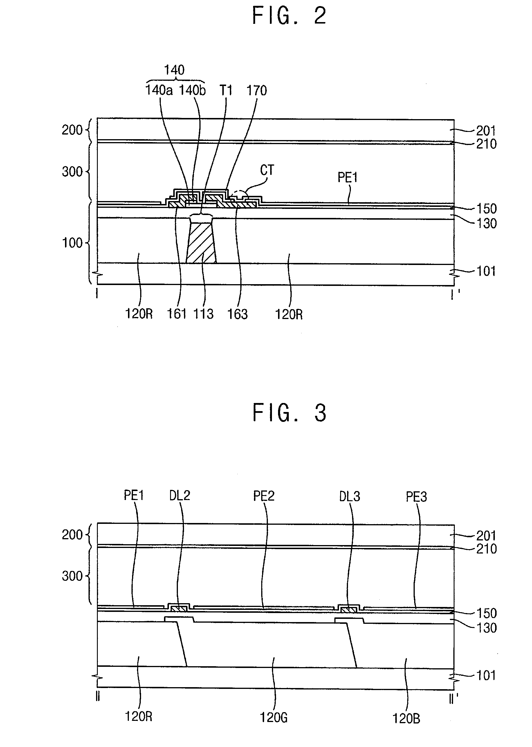
[0037]FIG. 1 is a plan view of a display panel according to Embodiment 1 of the present invention. FIG. 2 is a cross-sectional view taken along a line I-I′ of FIG. 1. FIG. 3 is a cross-sectional view taken along a line II-II′ of FIG. 1.

[0038]Referring to FIGS. 1 to 3, a display panel includes a display substrate 100, and an opposite substrate 200 coupled to the display substrate 100 to receive a liquid crystal layer 300.

[0039]The display substrate 100 includes a first base substrate 101. The first base substrate 101 includes a transparent material capable of transmitting light, for example, a glass substrate. The first base substrate 101 includes a red pixel area ‘R’, a green pixel area ‘G’ and a blue pixel area ‘B’.

[0040]Color filters 120R, 120G and 120B, a gate line GL, a gate electrode 113, an insulation layer 130, a semiconductor layer 140, data lines DL1, DL2 and DL3, a source electrode 163, a protective insulation layer 150 and pixel electrodes PE1, PE2 and PE3 are formed on t...

example embodiment 2

[0066]FIG. 9 is a cross-sectional view of a display substrate according to Embodiment 2 of the present invention. The display substrate according to this embodiment is substantially the same as the display substrate of Embodiment 1 except for at least a first metal wiring including a seed layer and a plating layer. Thus, the same reference numerals will be used to refer to the same or like parts as those described in Embodiment 1, and any further explanation concerning the above elements will be omitted.

[0067]Referring to FIGS. 1 and 9, the display substrate 100a includes color filters 120R, 120G and 120B, and a first metal wiring including a seed layer and a plating layer. The first metal wiring is provided in a trench T2 having an inverse-tapered shape formed between the adjacent color filters 120R, 120G and 120B.

[0068]The first metal wiring includes a gate line GL and a gate electrode of a switching element TR extruded from the gate line GL. For example, the gate electrode 113 ma...

example embodiment 3

[0077]FIG. 13 is a cross-sectional view of a display substrate according to Embodiment 3 of the present invention. The display substrate according to this embodiment is substantially the same as the display substrate of Embodiment 1 except for at least a trench of a forward-tapered shape. Thus, the same reference numerals will be used to refer to the same or like parts as those described in Embodiment 1, and any further explanation concerning the above elements will be omitted.

[0078]Referring to FIGS. 1 and 13, the display substrate 100b includes color filters 120R, 120G and 120B, and a first metal wiring. The first metal wiring is provided in a trench T3 having a forward-tapered shape, which is defined by at least one of the color filters 120R, 120G and 120B.

[0079]The first metal wiring includes a gate line GL and a gate electrode 113 of a switching element TR that is protruded from the gate line GL. For example, the gate electrode 113 may be provided in the trench T3 defined by th...


PUM

PropertyMeasurementUnit
thicknessaaaaaaaaaa
areaaaaaaaaaaa
coloraaaaaaaaaa

Abstract

A display substrate includes a plurality of color filters, a gate line, an insulation layer, a data line and a plurality of pixel electrodes. The color filters are formed on a base substrate. The gate line is formed in a trench defined by at least one of the color filters and extended along a first direction. The insulation layer is formed on the color filters and the gate line. The data line is formed on the insulation layer to be extended along a second direction crossing the first direction. The pixel electrodes are formed on the base substrate having the data line formed thereon. Therefore, a metal wiring is formed in a trench defined by color filters, so that the resistance of the metal wiring may be decreased and an aperture ratio may be enhanced.

Description

CROSS-REFERENCE TO RELATED APPLICATIONS[0001]This application claims priority under 35 U.S.C. § 119 to Korean Patent Application No. 2008-31070, filed on Apr. 3, 2008 in the Korean Intellectual Property Office (KIPO), the contents of which are herein incorporated by reference in their entirety.BACKGROUND OF THE INVENTION[0002]1. Field of the Invention[0003]Example embodiments of the present invention relate to a display substrate used in a liquid crystal display (LCD) device and a method of manufacturing the display substrate.[0004]2. Description of the Related Art[0005]A liquid crystal display (LCD) device includes a thin-film transistor (TFT) substrate, a color filter substrate and a liquid crystal layer interposed between the TFT substrate and the color filter substrate. The TFT substrate includes a wiring, a TFT, a pixel electrode, etc., that are formed on an insulation substrate to independently drive a plurality of pixels. The color filter substrate includes a color filter lay...

Claims


Application Information

Patent Timeline
Patent Type & Authority Applications(United States)
IPC IPC(8): G02F1/1335
CPCG02F1/133514G02F2201/40G02F2001/136222G02F1/136286G02F1/136222G02F1/1335G02F1/136
Inventor LEE, YOUNG-WOOKJO, GUG-RAEKIM, JANG-SOOYOUN, JAE-HYOUNGKIM, BYOUNG-JOOKIM, MIN-UKSON, KYOUNG-KEUN
Owner SAMSUNG DISPLAY CO LTD
Why Eureka
Try Eureka