Electro-optical device and electronic apparatus

a technology applied in the field of optical devices and electronic devices, can solve the problems of easy cracks in the light-shielding layer, and achieve the effect of lowering the resistance of metal wiring

Active Publication Date: 2019-05-02
SEIKO EPSON CORP
View PDF4 Cites 0 Cited by
  • Summary
  • Abstract
  • Description
  • Claims
  • Application Information

AI Technical Summary

Benefits of technology

[0014]The invention may employ an aspect in which a surface of the metal wiring at the first substrate side is formed of a metal film containing aluminum as the primary constituent. According to the aspect, the resistance of the metal wiring can be lowered. In this case as well, the third light-shielding layer and the second light-shielding layer prevent the return light from being reflected by the surface of the metal wiring at the first substrate side and emitted from the element substrate.

Problems solved by technology

Unfortunately, the light-shielding layer formed to fill spaces as in the configuration described in JP-A-2003-140129 makes cracks readily occur in the light-shielding layer due to the influence of stress generated in the light-shielding layer at the time of film formation, heat treatment, and the like.

Method used


Image

  • Electro-optical device and electronic apparatus
  • Electro-optical device and electronic apparatus
  • Electro-optical device and electronic apparatus

Examples


exemplary embodiment 1

Configuration of Electro-Optical Device

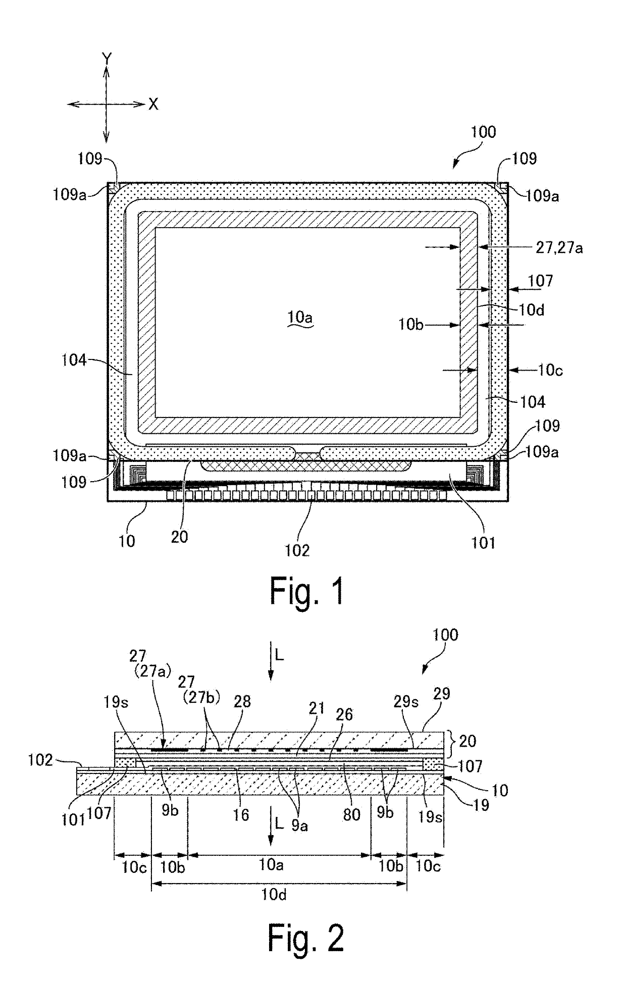
[0039]FIG. 1 is a plan view illustrating an electro-optical device 100 according to Exemplary Embodiment 1 of the invention. FIG. 2 is a cross-sectional view illustrating the electro-optical device 100 illustrated in FIG. 1. As illustrated in FIG. 1 and FIG. 2, the electro-optical device 100 includes an element substrate 10 and a counter substrate 20 bonded together with a sealing material 107 creating a predefined gap, where the element substrate 10 is opposed to the counter substrate 20. The sealing material 107 is provided in a frame-like shape in conformance with the outer edge of the counter substrate 20. An electro-optical layer 80 such as a liquid crystal layer is provided in an area surrounded by the sealing material 107 between the element substrate 10 and the counter substrate 20. Thus, the electro-optical device 100 is formed as a liquid-crystal device. The sealing material 107, which includes an adhesive having a photocurable proper...

exemplary embodiment 2

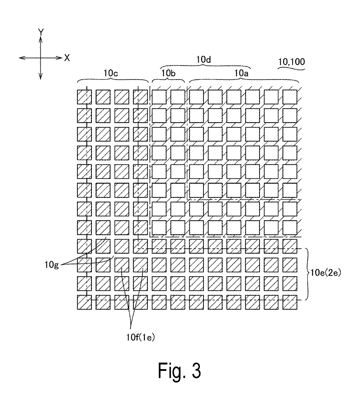
[0084]FIG. 15 is an explanatory diagram illustrating the electro-optical device 100 according to Exemplary Embodiment 2 of the invention, which is an explanatory view illustrating a cross-sectional configuration of the element substrate 10. Note that the basic configuration of Exemplary Embodiment 2 and Exemplary Embodiments 3, 4, and 5 described below is the same as the configuration of Exemplary Embodiment 1. Hence, common reference signs are given to common components and its descriptions are omitted. As illustrated in FIG. 15, in Exemplary Embodiment 2 as in Exemplary Embodiment 1, in the peripheral area 10c surrounding the pixel area 10d, there are formed the metal wiring 10e, the plurality of second light-shielding layers 10f overlapping in a plan view with the metal wiring 10e between the metal wiring 10e and the first substrate 19, and the third light-shielding layer 10h overlapping in a plan view with the second light-shielding interlayer area 10g between the metal wiring 1...

exemplary embodiment 3

[0087]FIG. 16 is an explanatory diagram illustrating the electro-optical device 100 according to Exemplary Embodiment 3 of the invention, which is an explanatory view illustrating a cross-sectional configuration of the element substrate 10. FIG. 17 is an explanatory view illustrating a planar configuration of the third light-shielding layer 10h and the second light-shielding layer 10f that are illustrated in FIG. 16. Note that FIG. 17 illustrates the peripheral area 10c of the element substrate 10 as viewed from the side opposed to the counter substrate 20.

[0088]As illustrated in FIG. 16, in Exemplary Embodiment 3 as in Exemplary Embodiment 1, in the peripheral area 10c surrounding the pixel area 10d, there are formed the metal wiring 10e, the plurality of second light-shielding layers 10f overlapping in a plan view with the metal wiring 10e between the metal wiring 10e and the first substrate 19, and the third light-shielding layer 10h overlapping in a plan view with the second lig...


PUM

PropertyMeasurementUnit
areaaaaaaaaaaa
reflectanceaaaaaaaaaa
light-shielding aaaaaaaaaa

Abstract

An element substrate of an electro-optical device includes, in a peripheral area surrounding a pixel area, a metal wiring provided at one surface side of a first substrate that is a substrate body, and a plurality of second light-shielding layers overlapping with the metal wiring between the first substrate and the metal wiring. A second light-shielding interlayer area overlapping with the metal wiring is present between the plurality of second light-shielding layers. A third light-shielding layer is formed in a manner overlapping in a plan view with the second light-shielding interlayer area between the first substrate and the metal wiring. Surfaces of the second light-shielding layer and the third light-shielding layer at the first substrate side have lower reflectance than a surface of the metal wiring at the first substrate side.

Description

BACKGROUND1. Technical Field[0001]The invention relates to an electro-optical device in which a metal wiring is formed in a peripheral area that surrounds a display area of an element substrate, and an electronic apparatus.2. Related Art[0002]A transmissive-type electro-optical device, used as a light valve and the like of a projection-type display apparatus, includes an element substrate provided with a pixel electrode having translucency at one surface side of a first substrate having translucency, and a counter substrate provided with a counter electrode having translucency on a surface of a second substrate at the element substrate side, the surface opposing to the one surface side of the first substrate, where an electro-optical layer is provided between the element substrate and the counter substrate. The electro-optical device modulates a light-source light by means of the electro-optical layer for each of the pixels and emits the light-source light while the light-source lig...

Claims


Application Information

Patent Timeline
Patent Type & Authority Applications(United States)
IPC IPC(8): G02F1/1362G02F1/1335G02F1/1347
CPCG02F1/136209G02F1/133528G02F1/1347G02F2001/133548G02F1/133512G02F2203/01G03B21/005G02F1/136295G02F1/133548
Inventor MASUI, JUNICHI
Owner SEIKO EPSON CORP
Why Eureka
Try Eureka