Circuit board and semiconductor integrated circuit module including the same

a technology of integrated circuit modules and circuit boards, which is applied in the direction of printed circuit details, cross-talk/noise/interference reduction, printed circuits, etc., can solve the problems of ground bounce noise (gbn), electromagnetic interference (emi), and degrading electrical communications both to and from the semiconductor integrated circuit modules

Inactive Publication Date: 2009-10-22
SK HYNIX INC
View PDF12 Cites 18 Cited by
  • Summary
  • Abstract
  • Description
  • Claims
  • Application Information

AI Technical Summary

Benefits of technology

[0011]In another aspect, a semiconductor integrated circuit module includes a circuit board, a memory control device configured to be mounted on the circuit board, and to generate and to output a plurality of differential signal pairs, a plurality of differential signal line pairs, each configured to be formed on the circuit board and to transmit a pair of the plurality of differential signal pairs, a

Problems solved by technology

As operational frequencies of semiconductor integrated apparatuses increase, ground bounce noise (GBN) has become important in semiconductor integrated circuit modules that include the semiconductor integrated apparatuses.
For example, the GBN generates a resonance between adjacent power supply layers and signal line layers within the semiconductor integrated circuit modules, thereby causing electromagnetic interference (EMI) and degrading the electrical communications both to and from the semiconductor integrated circuit modules.
However, since the semiconductor integrated

Method used


Image

  • Circuit board and semiconductor integrated circuit module including the same
  • Circuit board and semiconductor integrated circuit module including the same
  • Circuit board and semiconductor integrated circuit module including the same

Examples


Embodiment Construction

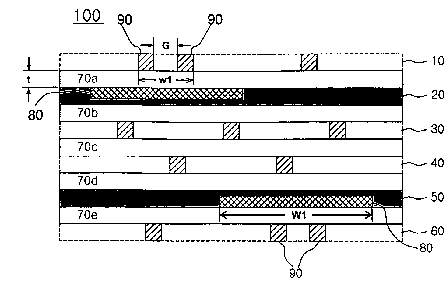
[0020]FIG. 1 is a cross-sectional view of an exemplary circuit board according to one embodiment. In FIG. 1, a circuit board 100 can be configured to include a plurality of signal line layers 10, 30, 40, and 60, a plurality of power supply layers 20 and 50, a plurality of insulating layers 70a to 70e, a plurality of electromagnetic bandgap (EBG) patterns 80, and a plurality of differential signal line pairs 90.

[0021]The plurality of signal line layers 10, 30, 40, and 60 can be stacked having predetermined gaps, such that they are not electrically connected to each other. Although the circuit board 100 is shown in FIG. 1 to include the four signal line layers 10, 30, 40, and 60, the structure of the circuit board 10 can have more or less than the four signal line layers 10, 30, 40, and 60. Here, the uppermost signal line layer 10 and the lowermost signal line layer 60 can be exposed at exterior side portions of the circuit board 100. Alternatively, only portions of the uppermost sign...


PUM


Abstract

A circuit board includes a plurality of differential signal line pairs, and a plurality of electromagnetic bandgap (EBG) patterns, each configured to be disposed to overlap the plurality of differential signal line pairs, wherein the EBG patterns are electrically insulated from the differential signal line pairs.

Description

CROSS-REFERENCES TO RELATED PATENT APPLICATION[0001]The present application claims priority under 35 U.S.C 119(a) to Korean Application No. 10-2008-0035229, filed on Apr. 16, 2008, in the Korean Intellectual Property Office, which is incorporated herein by reference in its entirety as set forth in full.BACKGROUND[0002]1. Technical Field[0003]The embodiments described herein relate to a semiconductor integrated circuit apparatus, and more particularly, to a circuit board having a semiconductor module mounted thereon.[0004]2. Related Art[0005]In general, a semiconductor package includes semiconductor chips mounted on a circuit board, such as a mother board or a printed circuit board (PCB) to constitute an integrated circuit module. Here, the circuit board includes an insulating substrate and a plurality of signal line layers that are disposed on the insulating substrate to provide electrical communications between the semiconductor chips.[0006]As operational frequencies of semiconduct...

Claims


Application Information

Patent Timeline
IPC IPC(8): H05K1/16H05K1/00
CPCH05K1/0236H05K1/0245H05K2201/09681H05K2201/09309H05K2201/09663H05K2201/09236H05K1/02
Inventor LEE, JUN HO
Owner SK HYNIX INC
Why Eureka
Try Eureka