Wiring board

a wiring board and wire technology, applied in the field of wiring boards, can solve the problems of not being able to make the surface of the wiring board b>200/b> small, not being able to efficiently arrange, and not being able to anticipate the pads b,

Inactive Publication Date: 2009-10-29
SHINKO ELECTRIC IND CO LTD
View PDF4 Cites 9 Cited by
  • Summary
  • Abstract
  • Description
  • Claims
  • Application Information

AI Technical Summary

Benefits of technology

[0013]Accordingly, embodiments of the present invention may provide a novel and useful wiring board solving one or more of the problems discussed above.

Problems solved by technology

However, in the related art wiring board 200, it is not expected that the pads 203 are efficiently arranged in an area as small as possible.
Therefore, it is difficult to make the surface of the wiring board 200 small.

Method used


Image

  • Wiring board
  • Wiring board
  • Wiring board

Examples


Embodiment Construction

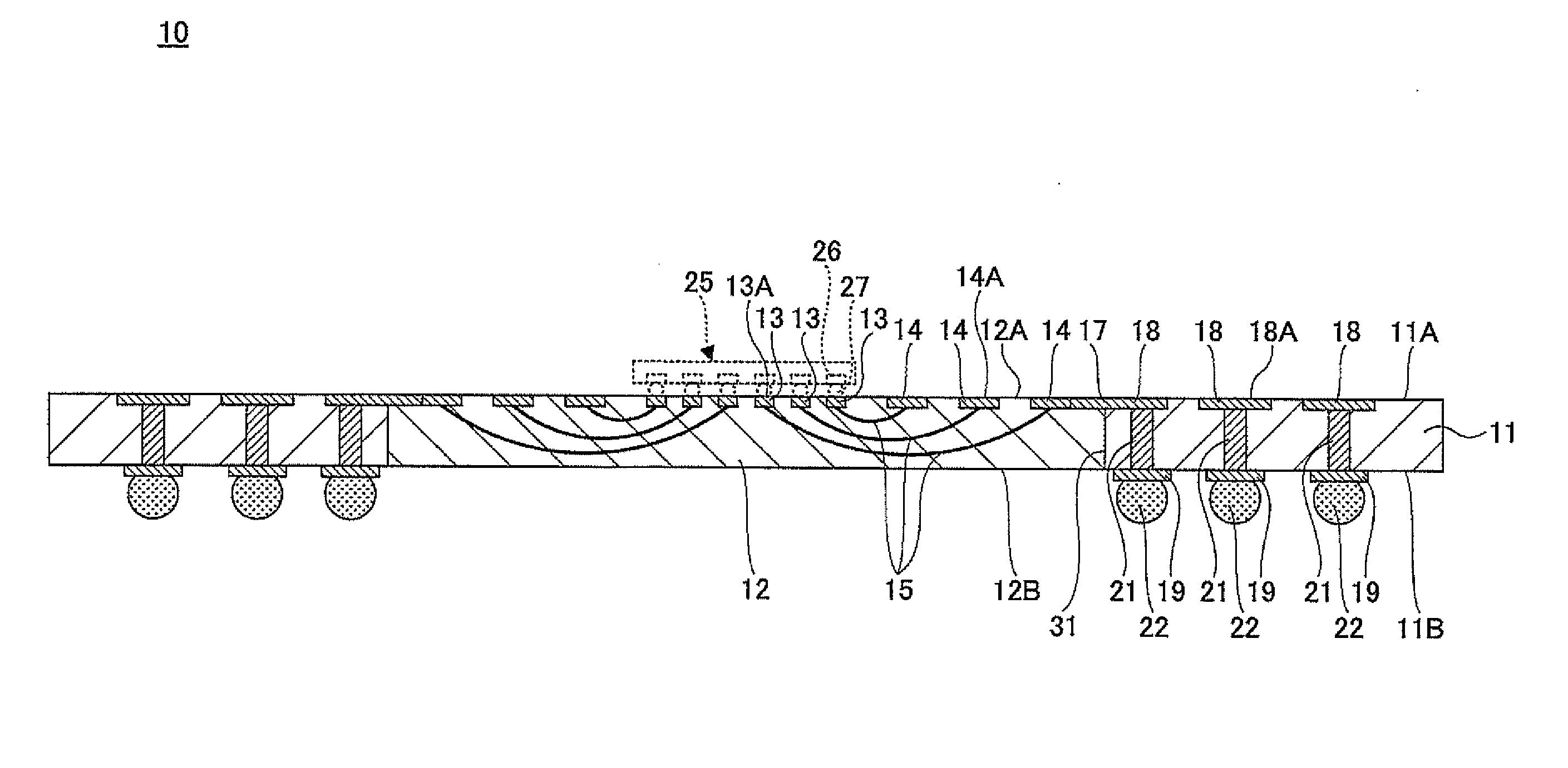
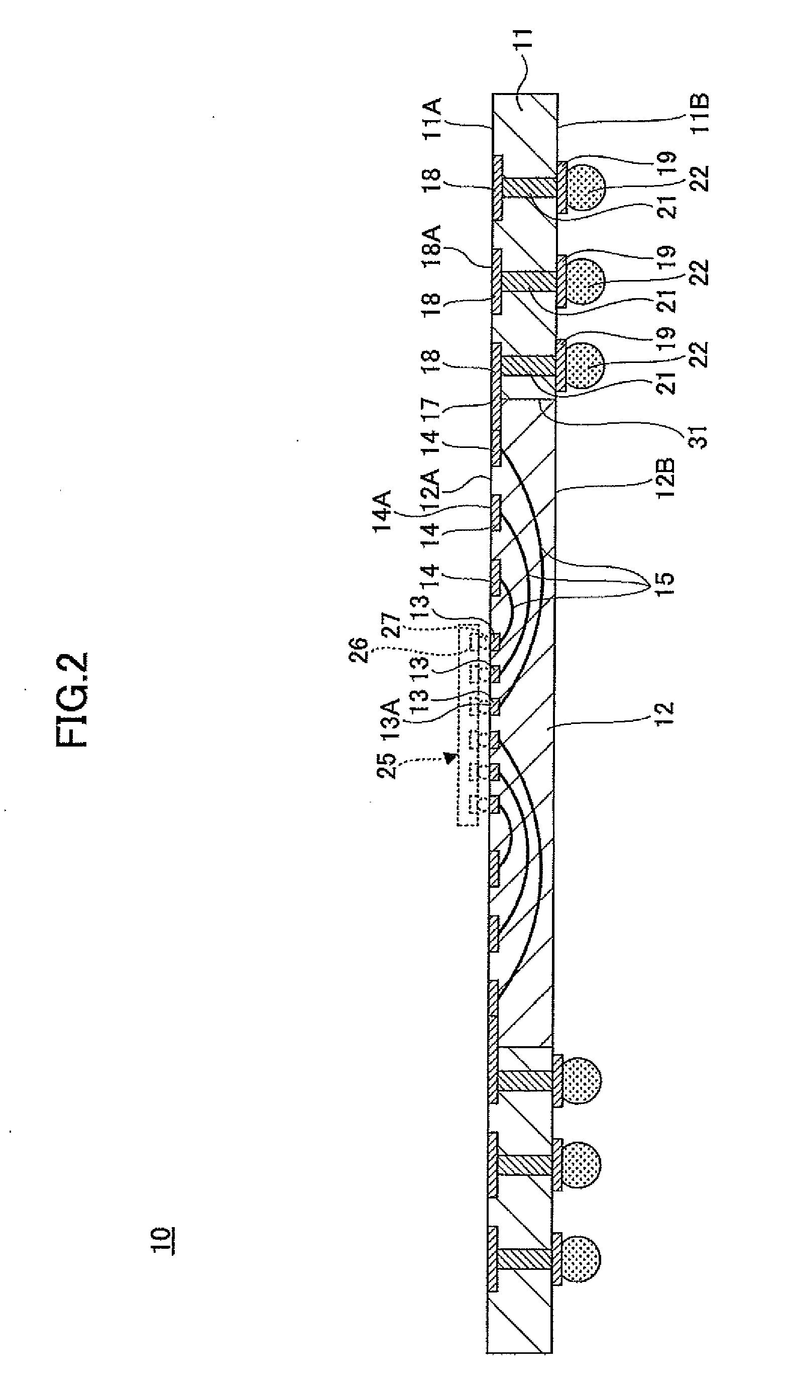
[0033]A description is given below, with reference to the FIG. 2 through FIG. 8 of embodiments of the present invention.

[0034]FIG. 2 is a cross-sectional view of a wiring board of an embodiment of the present invention.

[0035]As shown in FIG. 2, a wiring board 10 of the embodiment of the present invention includes a board main body 11, a resin member 12, chip connection pads 13, pads 14, conductive wires 15, lead wirings 17, piercing electrode pads 18, outside connection pads 19, and piercing electrodes 21.

[0036]The board main body 11 is a thin plate. A piercing part 31 is situated in the center part of the board main body 11. The piercing part 31 is a space configured to receive the resin member 12. As a material of the board main body 11, for example, a glass epoxy resin board can be used. The glass epoxy resin board comprises glass fibers covered with epoxy resin. The board main body 11 has a thickness of, for example, approximately 300 μm.

[0037]The resin member 12 has a plate sha...


PUM


Abstract

A wiring board includes a plate-shaped resin member; chip connection pads provided in the resin member, the chip connection pads having connection surfaces electrically connected to electrode pads provided on a semiconductor chip, the connection surfaces being situated in substantially the same plane as a first surface of the resin member, the first surface being a side where the semiconductor chip is mounted; pads provided in a portion of the resin member, the portion being situated outside an area where the chip connection pads are formed; lead wirings connected to the pads; and conductive wires sealed by the resin member, the conductive wires electrically connecting the chip connection pads and the pads to each other.

Description

CROSS-REFERENCE TO RELATED APPLICATIONS[0001]This patent application is based upon and claims the benefit of priority of Japanese Patent Application No. 2008-68533 filed on Mar. 17, 2008, the entire contents of which are incorporated herein by reference.BACKGROUND OF THE INVENTION[0002]1. Field of the Invention[0003]The present invention generally relates to wiring boards. More specifically, the present invention relates to a wiring board having pads electrically connected to chip connection pads via conductive wires.[0004]2. Description of the Related Art[0005]In related art wiring boards, there is a wiring board, for example, illustrated in FIG. 1, whereby electric connection reliability is improved and generation of cross-talk is prevented.[0006]FIG. 1 is a cross-sectional view of the related art wiring board.[0007]As shown in FIG. 1, a related art wiring board 200 includes a plate-shaped resin member 201, chip connection pads 202, pads 203, and conductive wires 205.[0008]The res...

Claims


Application Information

Patent Timeline
Patent Type & Authority Applications(United States)
IPC IPC(8): H05K1/11
CPCH01L23/498H05K2201/10674H01L23/49816H01L23/49822H01L23/49833H01L23/49838H01L2224/16H01L2924/01079H01L2924/15192H01L2924/15311H01L2924/19107H05K1/111H05K3/103H05K3/222H05K2201/09418H05K2201/09709H05K2201/10287H01L23/49811H01L2224/05571H01L2224/05573H01L2924/00014H01L2224/05599
Inventor KATAGIRI, FUMIMASATOKUTAKE, YASUEKOIZUMI, NAOYUKISUGANUMA, SHIGEAKIHORIUCHI, MICHIO
Owner SHINKO ELECTRIC IND CO LTD
Why Eureka
Try Eureka