Methods and apparatus for transporting substrate carriers

a technology of substrate carriers and transport methods, applied in lighting and heating apparatus, charge manipulation, furnaces, etc., can solve the problem of increasing the manufacturing cost per substrate, and achieve the effect of efficient and reliable arrangemen

Active Publication Date: 2006-07-18
APPLIED MATERIALS INC
View PDF147 Cites 52 Cited by
  • Summary
  • Abstract
  • Description
  • Claims
  • Application Information

AI Technical Summary

Benefits of technology

[0022]The methods and apparatus of the present invention provide for an efficient and reliable arrangement for transporting substrate carriers within one or more semiconductor device manufacturing facilities.

Problems solved by technology

The substrates present in the fabrication facility as WIP may represent a large investment of working capital, which tends to increase the per substrate manufacturing cost.

Method used


Image

  • Methods and apparatus for transporting substrate carriers
  • Methods and apparatus for transporting substrate carriers
  • Methods and apparatus for transporting substrate carriers

Examples


Embodiment Construction

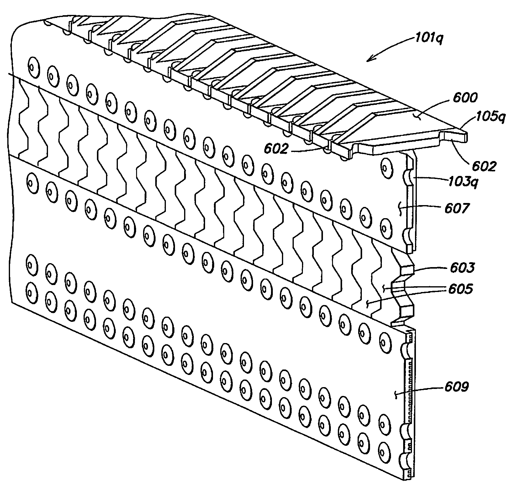
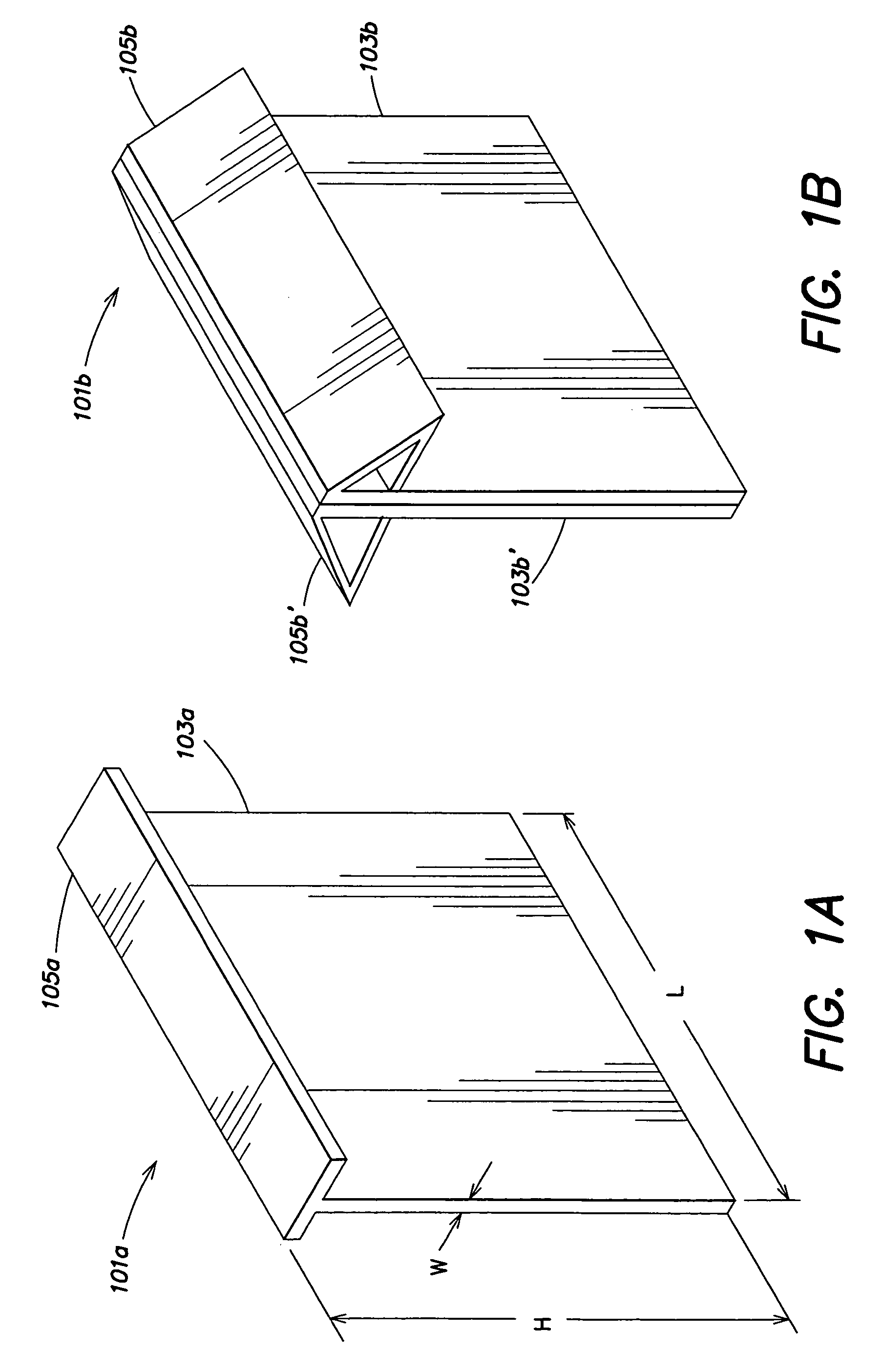
[0047]In accordance with at least one aspect of the invention, an inventive conveyor system is provided for transporting substrate carriers between one or more processing tools of a semiconductor device manufacturing facility. The inventive conveyor system may include a ribbon of stainless steel or a similar material that forms a closed loop within at least a portion of the semiconductor device manufacturing facility and that transports substrate carriers therein. By orienting the ribbon so that a thick portion of the ribbon resides within a vertical plane and a thin portion of the ribbon resides within a horizontal plane, the ribbon is flexible in the horizontal plane and rigid in the vertical plane. Such a configuration allows the inventive conveyor to be constructed and implemented inexpensively. For example, the ribbon requires little material to construct, is easy to fabricate and, due to its vertical rigidity / strength, can support the weight of numerous substrate carriers with...


PUM


Abstract

According to a first aspect, a first conveyor system is provided that is adapted to deliver substrate carriers within a semiconductor device manufacturing facility. The first conveyor system includes a ribbon that forms a closed loop along at least a portion of the semiconductor device manufacturing facility. The ribbon is adapted to (1) be flexible in a horizontal plane and rigid in a vertical plane; and (2) transport a plurality of substrate carriers within at least a portion of the semiconductor device manufacturing facility. Numerous other aspects are provided, as are systems, methods and computer program products in accordance with these and other aspects.

Description

[0001]The present application claims priority from U.S. Provisional Patent Application Ser. No. 60 / 443,087, filed Jan. 27, 2003, which is hereby incorporated by reference herein in its entirety.FIELD OF THE INVENTION[0002]The present invention relates generally to semiconductor device fabrication systems, and is more particularly concerned with transportation of substrate carries within a fabrication facility.CROSS REFERENCE TO RELATED APPLICATIONS[0003]The present application is related to the following commonly-assigned, co-pending U.S. Patent Applications, each of which is hereby incorporated by reference herein in its entirety:[0004]U.S. patent application Ser. No. 10 / 650,310, filed Aug. 28, 2003 and titled “System For Transporting Substrate Carriers”;[0005]U.S. patent application Ser. No. 10 / 650,312, filed Aug. 28, 2003 and titled “Method and Apparatus for Using Substrate Carrier Movement to Actuate Substrate Carrier Door Opening / Closing”;[0006]U.S. patent application Ser. No. ...

Claims


Application Information

Patent Timeline
Patent Type & Authority Patents(United States)
IPC IPC(8): B65G17/02H01L21/677B65G49/07H01L21/68
CPCB65G17/20B65G37/02H01L21/67706H01L21/6773H01L21/67769H01L21/67778H01L21/67727B65G2201/0297Y10S414/135A01K93/00A01K97/00
Inventor RICE, MICHAEL R.LOWRANCE, ROBERT B.ELLIOTT, MARTIN R.HUDGENS, JEFFREY C.ENGLHARDT, ERIC A.
Owner APPLIED MATERIALS INC
Why Eureka
Try Eureka