Image pickup device that is provided with peripheral circuits to prevent chip area from being increased, and image pickup apparatus

a peripheral circuit and pickup device technology, applied in the direction of radio frequency control devices, instruments, television systems, etc., can solve the problems of non-uniform dark current in a screen-associated region, variation in the capacity value of fd, prnu (photo response non-uniformity) and dsnu (dark signal non-uniformity), etc., to prevent the increase of the chip area of the peripheral circuit and suppress the increase of the chip area

Active Publication Date: 2013-02-07
CANON KK
View PDF8 Cites 46 Cited by
  • Summary
  • Abstract
  • Description
  • Claims
  • Application Information

AI Technical Summary

Benefits of technology

[0017]The present invention provides an image pickup device which suppresses an increase in chip area of peripheral circuits without d

Problems solved by technology

However, in the technique described in Japanese Patent Laid-Open Publication No. 2008-211220, chips are connected via the floating diffusions in each of which the signal is faint among all signals within the pixel, and hence variation in the manufacturing of products of the FD results in variation in the capacity value of the FD, which causes PRNU

Method used


Image

  • Image pickup device that is provided with peripheral circuits to prevent chip area from being increased, and image pickup apparatus
  • Image pickup device that is provided with peripheral circuits to prevent chip area from being increased, and image pickup apparatus
  • Image pickup device that is provided with peripheral circuits to prevent chip area from being increased, and image pickup apparatus

Examples


first embodiment

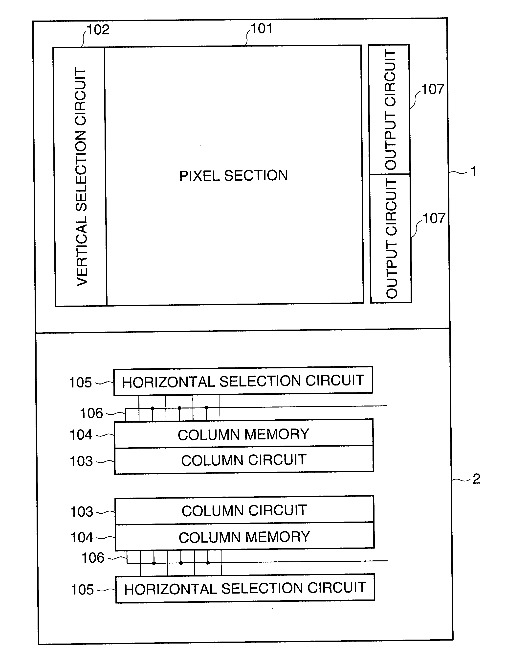
[0055]FIG. 1 is a block diagram useful in explaining the overall configuration of an image pickup device according to the present invention. It is assumed that in actuality, illustrated areas 1 and 2 overlap in a vertical direction.

[0056]In FIG. 1, the image pickup device includes a pixel section 101, a vertical selection circuit 102 which selects at least one of rows of pixels in the pixel section 101, and column circuits 103 each of which reads out signals from pixels on a pixel row in the pixel section 101 selected by the vertical selection circuit 102, and performs predetermined processing on the read signals. The image pickup device further includes column memories 104 each of which holds signals processed by the column circuits 103, on a column basis, horizontal selection circuits 105 each of which selects a signal held in the associated column memory 104, and output signal lines 106 each of which reads out signals from a column selected by the horizontal selection circuit 105...

second embodiment

[0078]FIG. 8 is a view showing a cross-sectional structure of an image pickup device according to the present invention. The same components as those shown in FIGS. 2 and 5 are denoted by same reference numerals, and description thereof is omitted.

[0079]In the second embodiment shown in FIG. 8, the area 1 and the area 2 are formed on the front side (first side or second side) and the back side (first side or second side) of the semiconductor substrate 501, respectively. In the present embodiment, a description will be given assuming that a side on which the area 1 is formed is the front side, and a side on which the area 2 is formed is the back side. A protective layer 801 protects the interconnection layer 505 on the back side. Plugs 802 electrically connect between the front side and the back side.

[0080]Further, although in the above-described embodiments, the description has been given of the area 1 and the area 2, the areas are not limited to two, but may be divided into a plura...

third embodiment

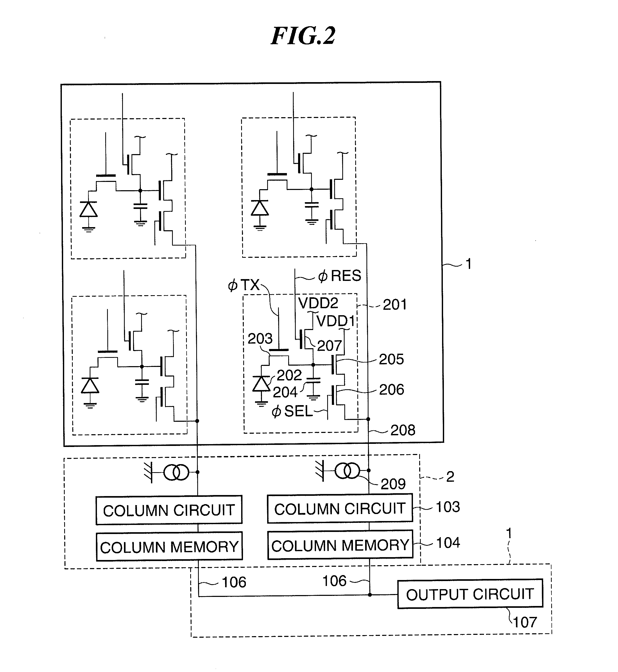
[0087]FIG. 11 is a diagram showing a configuration of a pixel and a circuit configuration for reading out a signal from the pixel, in an image pickup device according to the present invention. The area 1 is a chip including circuits formed on the first semiconductor substrate, and the area 2 is a chip including circuits formed on the second semiconductor substrate.

[0088]The area 1 mainly includes the pixels 201, and the area 2 mainly includes the column circuit for processing a signal from each pixel 201.

[0089]The area 1 is formed by arranging a plurality of the pixels 201 in a two-dimensional array as a pixel array which provides a two-dimensional image. Each pixel 201 can be configured to include the photo diode (hereinafter also referred to as the “PD”) 202, the transfer switch 203, the floating diffusion (hereinafter also referred to as the “FD”) 204, the MOS amplifier 205, the selection switch 206, and the reset switch 207.

[0090]The PD 202 functions as a photoelectric conversio...


PUM


Abstract

An image pickup device which suppresses an increase in chip area of peripheral circuits without degrading the performance of a pixel section and makes it possible to prevent costs from being increased. The image pickup device includes a first semiconductor substrate and a second semiconductor substrate. A pixel section includes photo diodes each for generate electric charges by photoelectric conversion, floating diffusions each for temporarily storing the electric charges generated by the photo diode, and amplifiers each connected to the floating diffusion, for outputting a signal dependent on a potential of the associated floating diffusion. Column circuits are connected to vertical signal lines, respectively, for performing predetermined processing on signals output from the pixel section to vertical signal lines.

Description

BACKGROUND OF THE INVENTION[0001]1. Field of the Invention[0002]The present invention relates to an image pickup device and an image pickup apparatus, and more particularly to a technique concerning a circuit forming the image pickup device.[0003]2. Description of the Related Art[0004]Conventionally, there has been developed an image pickup apparatus, such as a digital camera and a digital video camera, which records a shot image using a CMOSAPS (complementary metal oxide semiconductor active pixel sensor) as an image pickup device. The image pickup device includes a pixel section and a peripheral circuit section. The peripheral circuit section reads out a signal from each pixel and is output to the outside as an image signal. The pixel section performs photoelectric conversion by photo diodes, and a pixel circuit formed in the pixel section reads out a signal obtained by photoelectric conversion to the peripheral circuit section.[0005]In recent years, as the pixel becomes finer, as...

Claims


Application Information

Patent Timeline
IPC IPC(8): H01L27/148H01L27/146H04N5/335
CPCH01L27/14634H01L27/14636H04N5/3742H01L27/14643H01L27/1464H04N25/767H01L27/14638H04N25/79H04N25/76H01L27/146H04N25/77H04N25/75
Inventor KISHI, TAKAFUMI
Owner CANON KK
Why Eureka
Try Eureka