Electronic device with phononic crystal structure

a technology of phononic crystals and electronic devices, applied in the field of electronic devices with phononic crystal structures, can solve problems such as user discomfort and generation of loud noises

Inactive Publication Date: 2009-11-19
HON HAI PRECISION IND CO LTD
View PDF23 Cites 24 Cited by
  • Summary
  • Abstract
  • Description
  • Claims
  • Application Information

AI Technical Summary

Problems solved by technology

Generally, the fan generates a loud noise during ...

Method used


Image

  • Electronic device with phononic crystal structure
  • Electronic device with phononic crystal structure
  • Electronic device with phononic crystal structure

Examples


Embodiment Construction

[0011]Embodiments will now be described in detail below with reference to the drawings.

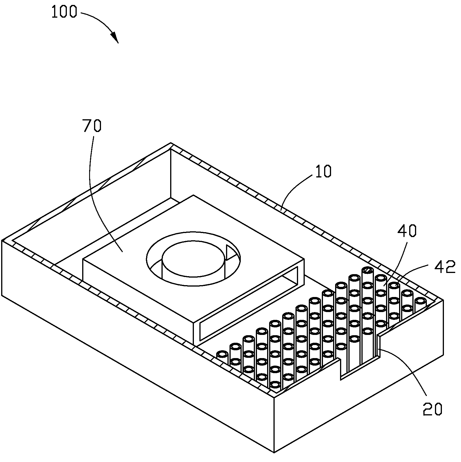
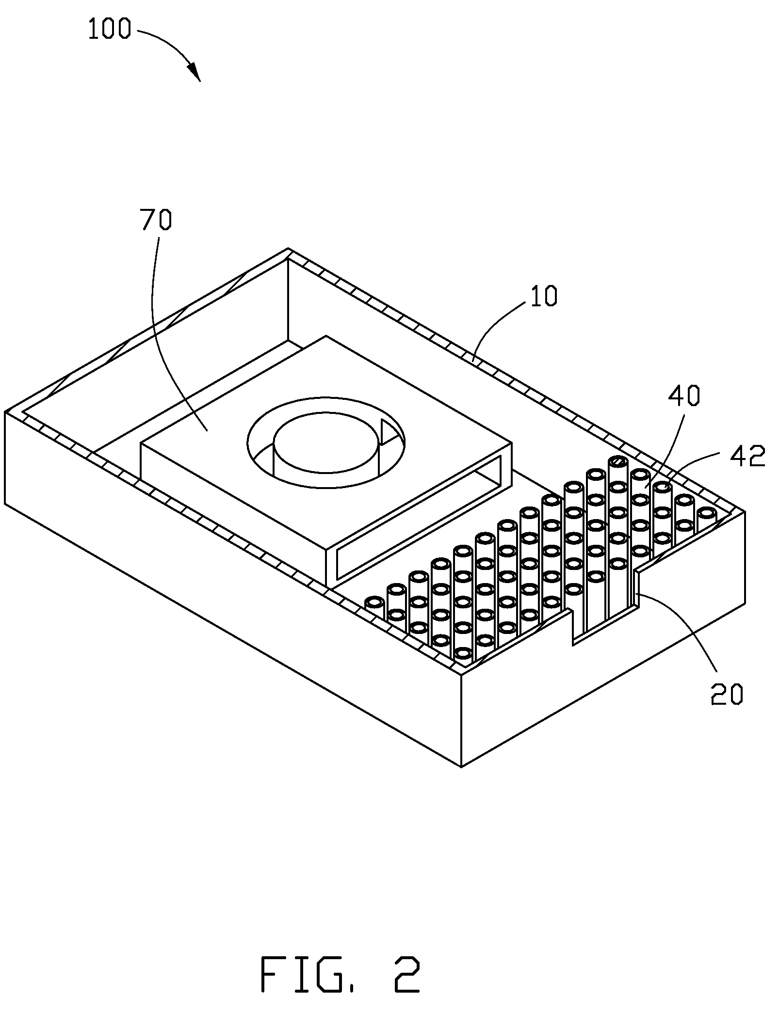
[0012]Referring to FIGS. 1-3, an electronic device 100 in accordance with an exemplary embodiment is shown. The electronic device 100 includes a housing 10, a fan 70 and a two-dimensional phononic crystal structure 40. Other electronic components of the electronic device 100 are not shown.

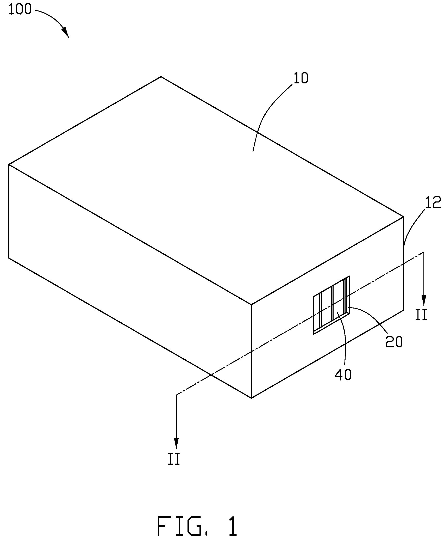
[0013]The housing 10 includes a bottom plate 14, a side plate 12 connected with the bottom plate 14. The bottom plate 14 includes a surface 142. The side plate 12 defines a heat-dissipating opening 20 therein.

[0014]The fan 70 is disposed on the surface 142 of the bottom plate 14 and is received in the housing 10. The fan 70 is configured for dissipating heat from the electronic device 10.

[0015]The phononic crystal structure 40 is formed on the surface 142 of the bottom plate 14. The phononic crystal structure 40 is positioned between the fan 70 and the side plate 12, and is adjacent to the heat-dissipating openin...


PUM


Abstract

An exemplary electronic device includes a housing and a plurality of parallel bars. The housing defines a chamber therein and a heat-dissipating opening at one side thereof. The bars are configured for abating noises, and are received in the chamber and adjacent to the heat-dissipating opening. The bars are arranged in a two-dimensional crystal lattice.

Description

BACKGROUND[0001]1. Technical Field[0002]The present invention relates to an electronic device with a phononic crystal structure.[0003]2 Description of Related Art[0004]Many kinds of electronic devices, such as projectors, personal computers, have been widely used in daily life. Electronic devices usually employ a fan to dissipate heat. Generally, the fan generates a loud noise during functioning, which makes cause discomfort to the users.[0005]Therefore, a new electronic device is desired to overcome the above mentioned problems.BRIEF DESCRIPTION OF THE DRAWINGS[0006]Many aspects of the embodiments can be better understood with references to the following drawings. The components in the drawings are not necessarily drawn to scale, the emphasis instead being placed upon clearly illustrating the principles of the present embodiments. Moreover, in the drawings, like reference numerals designate corresponding parts throughout the several views.[0007]FIG. 1 is a schematic, isometric view...

Claims


Application Information

Patent Timeline
IPC IPC(8): H05K7/20
CPCG06F1/182H05K7/20136G06F1/20
Inventor CHOU, TAI-HSU
Owner HON HAI PRECISION IND CO LTD
Why Eureka
Try Eureka