Design-For-Test-Aware Hierarchical Design Planning

Inactive Publication Date: 2009-11-19
SYNOPSYS INC
View PDF6 Cites 13 Cited by
  • Summary
  • Abstract
  • Description
  • Claims
  • Application Information

AI Technical Summary

Benefits of technology

[0023]A method of performing DFT-aware design planning can advantageously facilitate automatic updates to scan data, thereby significantly improving resource management. In this method, a DFT-inserted netlist for an integrated circuit (IC)

Problems solved by technology

Therefore, although scan cells are necessary to provide chip testability, their presence on the chip is otherwise a liability.
However, current tool sets cannot take advantage of this flexibility, as explained below.
However, this alternative is not commercially viable (or perh

Method used


Image

  • Design-For-Test-Aware Hierarchical Design Planning
  • Design-For-Test-Aware Hierarchical Design Planning
  • Design-For-Test-Aware Hierarchical Design Planning

Examples


Example

DETAILED DESCRIPTION OF THE FIGURES

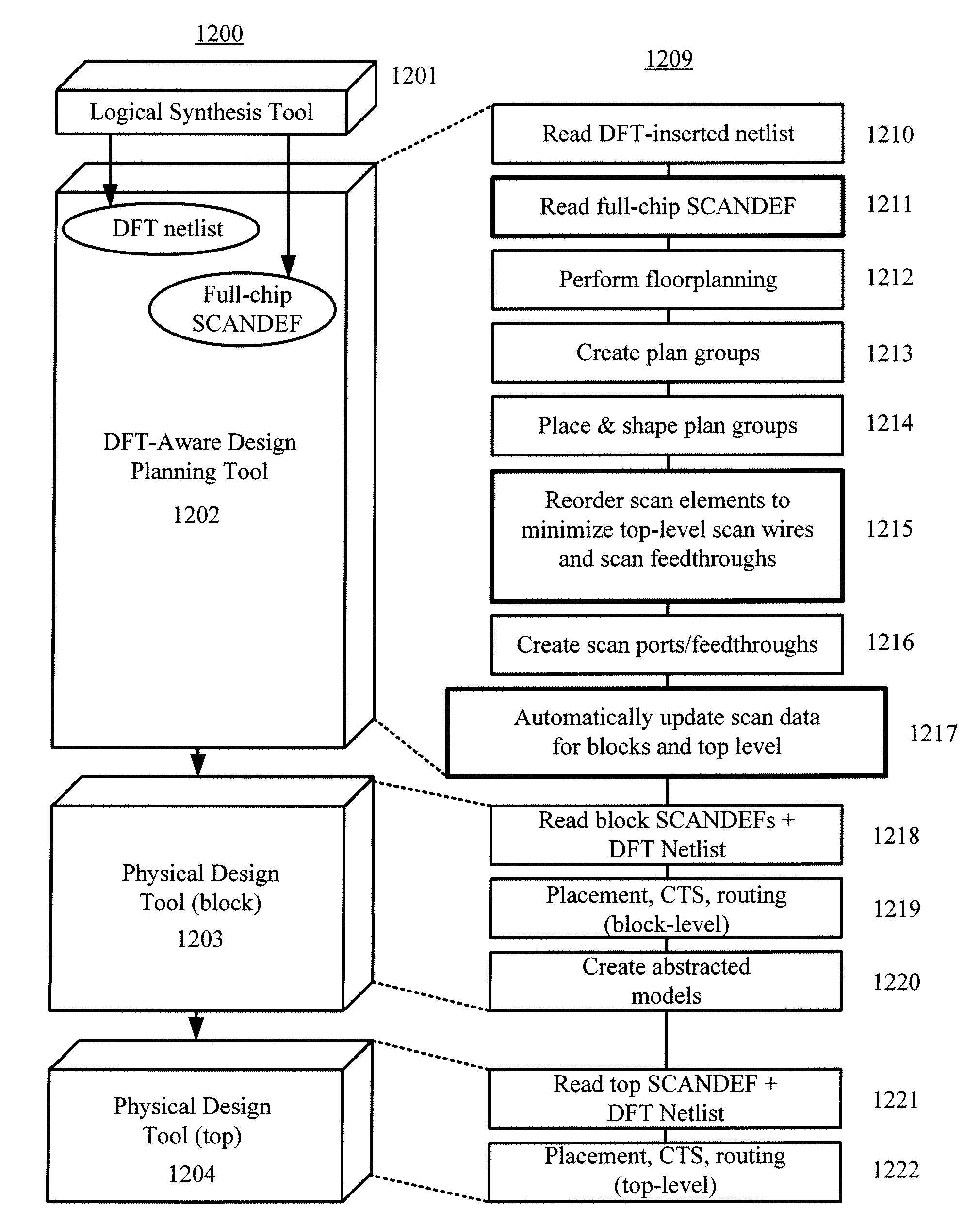
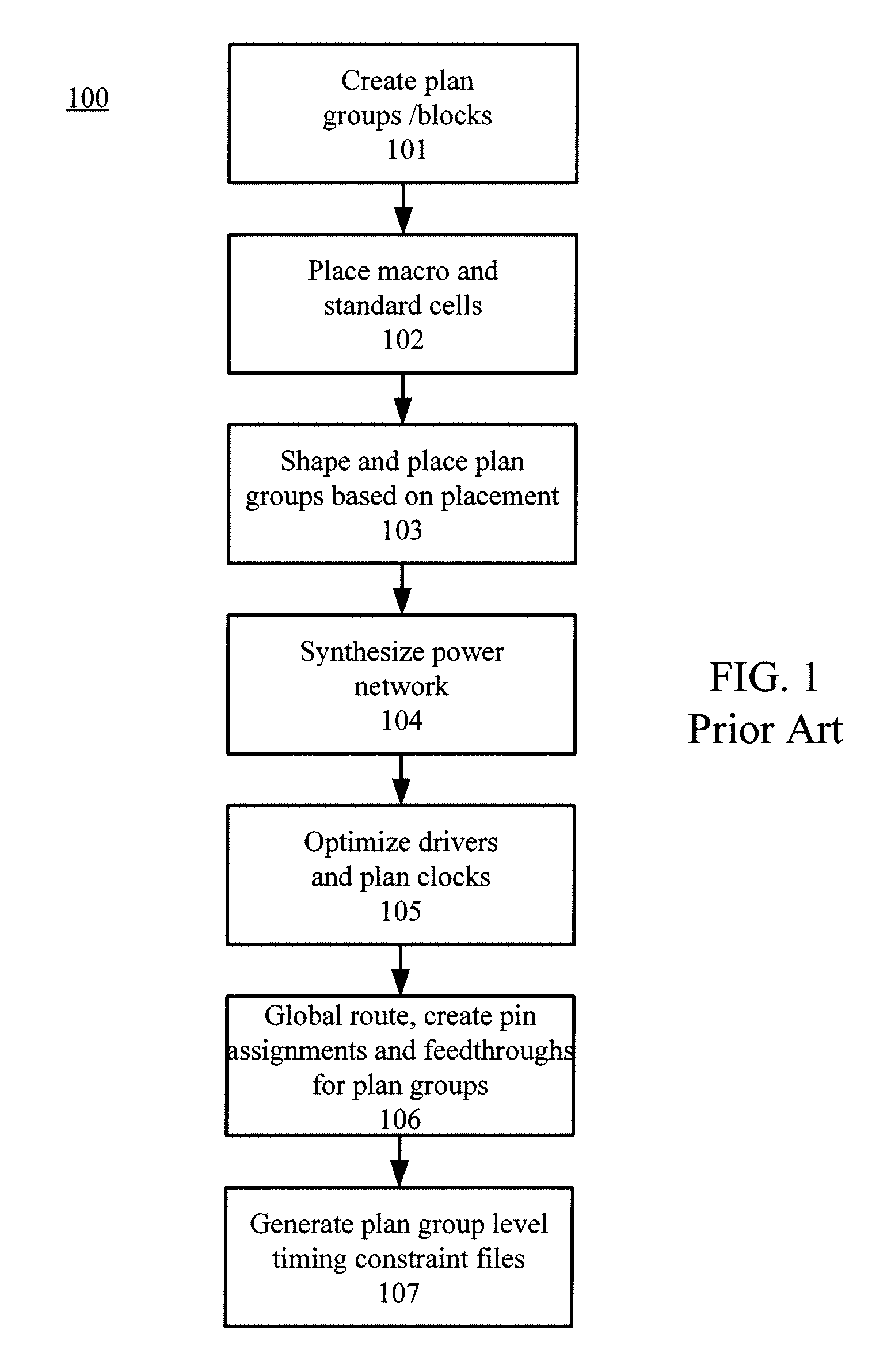
[0052]Current design planning typically results in the physical hierarchy being the same as the logical hierarchy. This enforced correspondence can cause sub-optimal physical design because logical connections are generally not physically friendly, e.g. an excessive number of top-level scan wires and feedthroughs. Thus, current design planning needs improvement.

[0053]In accordance with one feature of a DFT-aware design planning technique, full-chip scan data can be used to minimize top-level scan wires and feedthroughs. Corresponding block-level and top-level scan data can be advantageously updated automatically. Therefore, as explained in more detail below, a DFT-aware design planning technique can provide significant improvements in tool and resource efficiency.

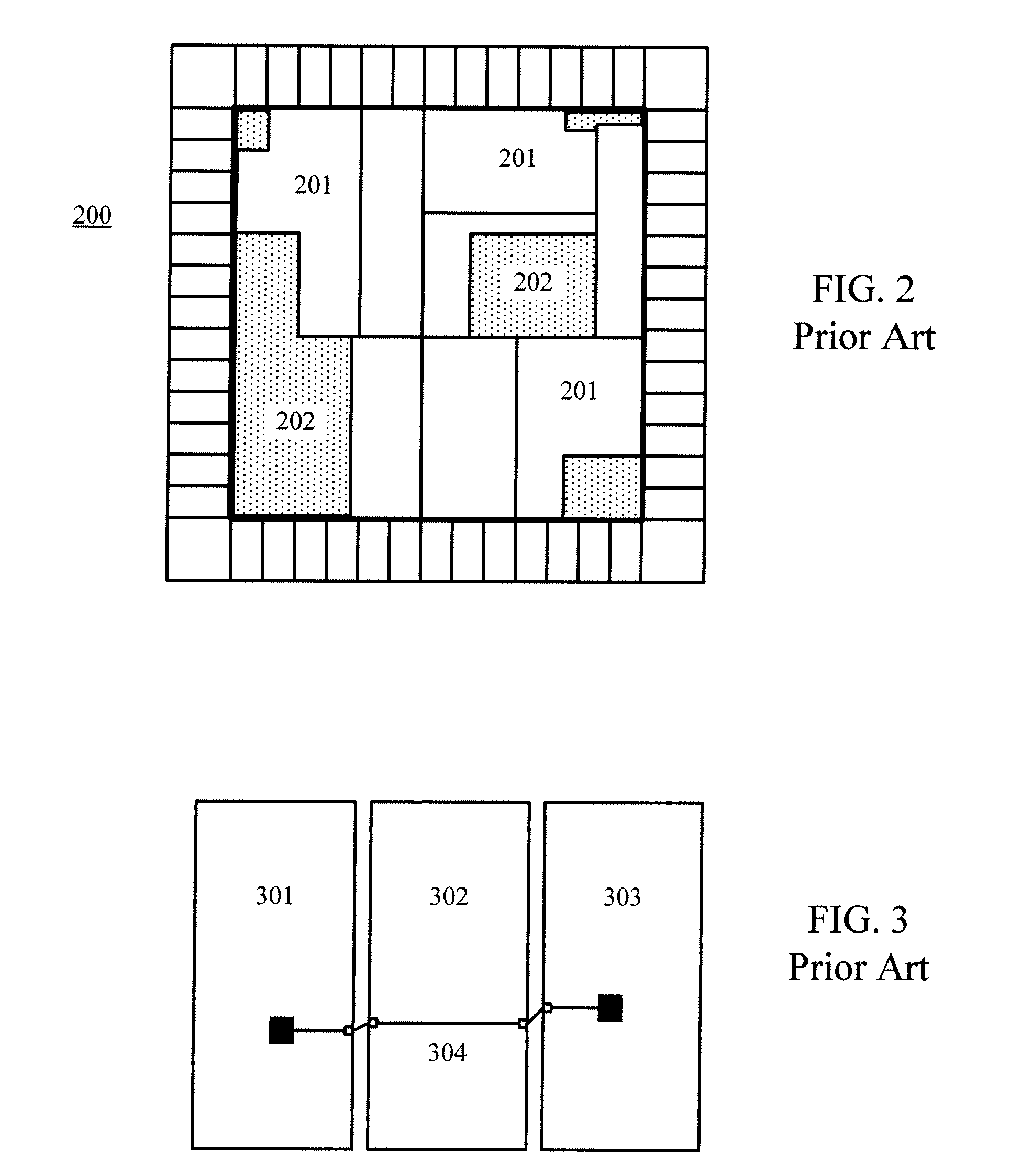
[0054]FIG. 8 illustrates one type of problem that can be minimized by a DFT-aware design planning technique. Specifically, as shown in FIG. 8, a scan chain 800 (represented by a dotted wir...


PUM


Abstract

Full-chip scan data can be advantageously used during design planning to minimize top-level scan wires and scan feedthroughs. The scan cells can be reordered using a modified cost function to promote connecting all scan cells in one plan group before crossing to a scan cell in another plan group. The modified cost function can take into account penalty parameters. The penalty parameters can include at least one of: membership in a plan group or a top-level physical hierarchy, size of a plan group, FLOATING/ORDERED scan element in scan data, location of endpoints of an ORDERED list, location of endpoints of a macro, and membership in a plan group containing a STOP point. Scan data, at the block-level and at the top-level, can be automatically updated to reflect the plan groups and optimized scan chains.

Description

BACKGROUND OF THE INVENTION[0001]1. Field of the Invention[0002]The present invention relates to scan cells that are used to test a digital integrated circuit (IC) and in particular to using DFT-aware design planning information to optimize top-level scan wires and scan feedthroughs during design planning and then automatically update block-level and top-level scan chain information.[0003]2. Related Art[0004]In general, both logical and physical design tools can be used to create a physical design for an IC. Logical tools can determine the logic necessary to implement the desired functionalities of the IC. Physical design tools can place that logic on the IC in a manner that optimizes chip area and performance. Logical tools are only aware of logical hierarchy. Current physical design tools are aware of logical hierarchy and physical hierarchy. Both the logical and physical design tools use significant resources (e.g. memory and CPU time).[0005]One way to reduce the resources used b...

Claims


Application Information

Patent Timeline
IPC IPC(8): G06F17/50
CPCG06F2217/14G06F17/505G06F30/327G06F30/333
Inventor CHIEN, HUNG-CHUNMATHEW, BENTAKKARS, PADMASHREELIU, BANGTAI, CHANG-WEIXIONG, XIAO-MINGYEAP, GARY K.
Owner SYNOPSYS INC
Why Eureka
Try Eureka