This helps you quickly interpret patents by identifying the three key elements:
Problems solved by technology
Method used
Benefits of technology
[0018]In this way, by providing the optical waveguide in the first gap, the operation stability can be increased. Then, the first gap width is made smaller than the second gap width, and the optical waveguide is provided in the narrower first gap and is not provided in the wider second gap. Since the first gap is narrower in width, the electric field intensity applied to the optical waveguide in the gap is large, and the drive voltage required for predetermined phase modulation decreases compared with a case of an ordinary symmetrical CPW electrodes. On the other hand
Problems solved by technology
Further, since it does not have a structure as coplanar electrodes in which a signal electrode is arranged between ground electrodes, it has a defect that electric field confinement is weak, due to an discontinuous points in a bent portion of the signal electrode, a connection portion to a radio frequency coaxial cable, and the lik
Method used
Image
Click on the blue label to locate the original text in one second.
Reading with bidirectional positioning of images and text.
Examples
Example
First Example
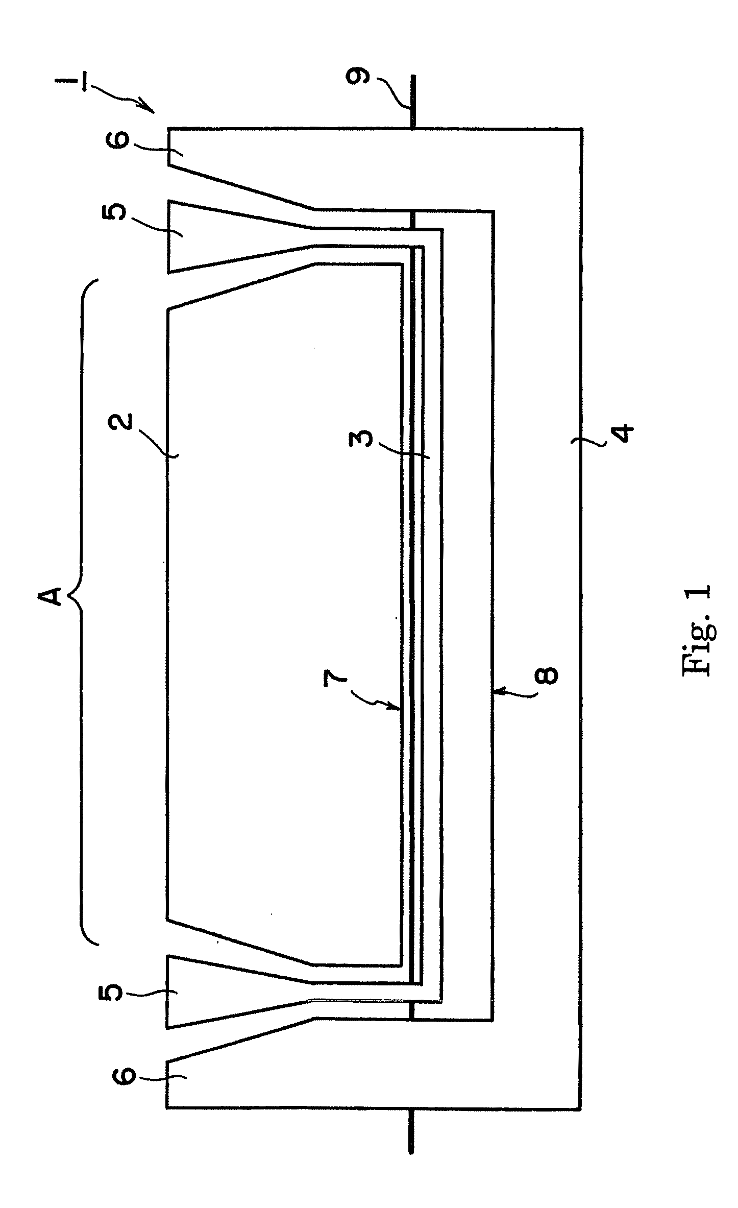
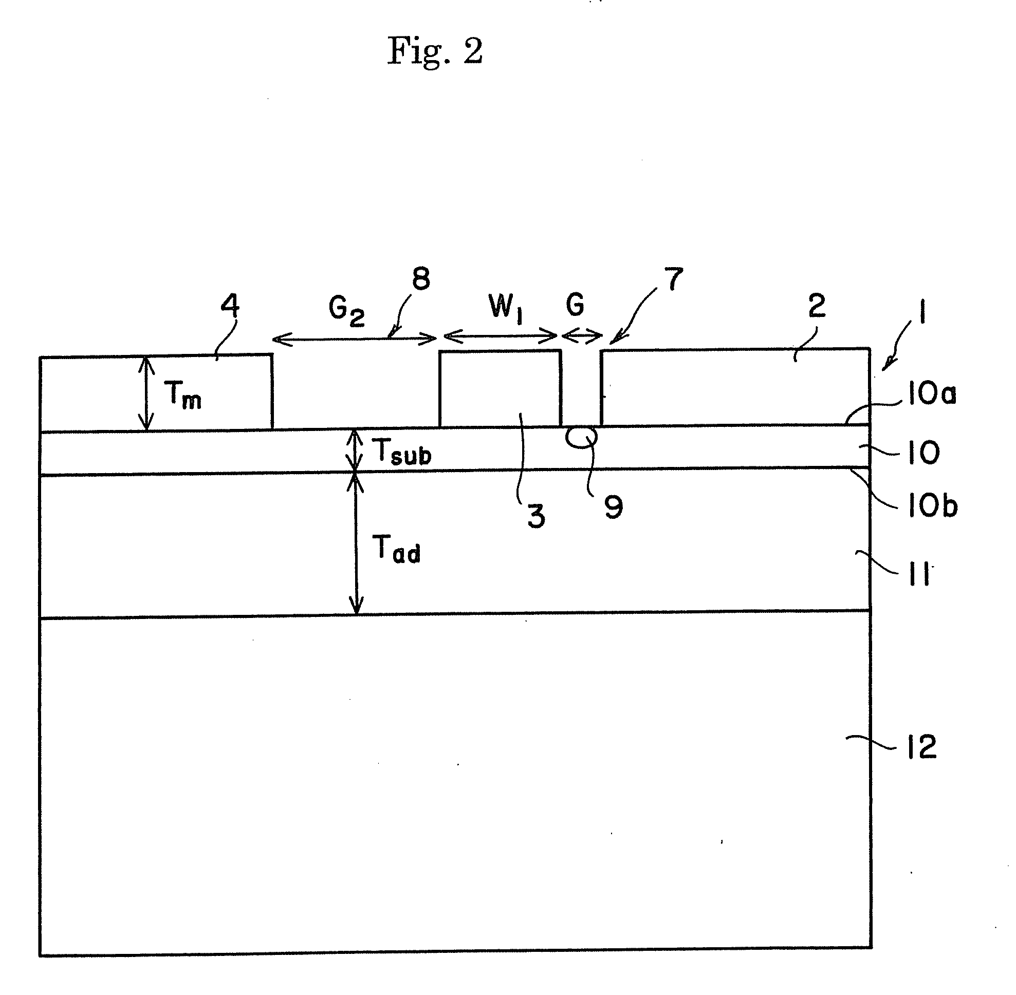
[0068]The optical phase modulator 1 as shown in FIGS. 1 and 2 was produced, and a phase modulation experiment was carried out. Sizes are set as follows (refer to FIG. 2).
G1=16 μm, G2=92 μm, W=38 μm, Tm=20 μm,
[0069]Tsub=7.0 μm, Tad=50 μm, and relative permittivity of the low dielectric constant layer 11: 4.0.
[0070]As the electric-optical substrate 10, an X-cut lithium niobate substrate was used. With this structure, the effective refractive index of microwave was 2.2, and the microwave and light are velocity-matched. The characteristic impedance was 43 Ω. Moreover, the half-wave voltage Vπ decreased down to 3.3V when the interaction-length of the electrodes was 32 mm.
Example
Second Example
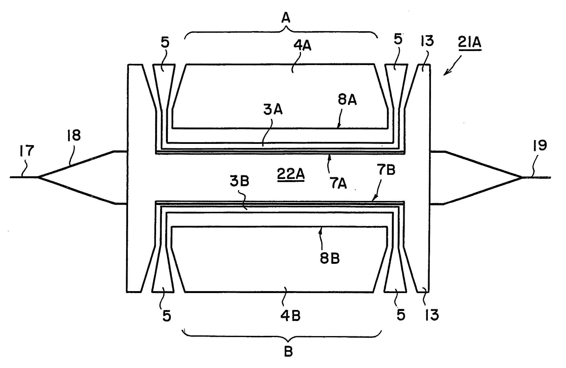
[0071]The optical phase modulator 21 as shown in FIGS. 3 and 4 was produced, and a phase modulation experiment was carried out. It should be noted that the following dimensions were set.
W=40 μm, G1=16.5 μm, G2=90 μm,
WGND=WGND2=WGND3=100 μm, Tsub=7 μm,
electrode thickness Tm=17 μm, and electrode interaction length L=3.2 cm.
[0072]As the electric-optical substrate 1, an X-cut lithium niobate substrate was used. With this structure, the effective refractive index of microwave was 2.2, and the microwave and light are velocity-matched. The following data were obtained under these conditions.
[0073]Electrode conductor loss α=0.33 dB·cm−1·GHz−1 / 2
[0074]Characteristic impedance Z=41 Ω
[0075]Half wave voltage Vπ=3.4 V
[0076]Product of half wave voltage and interaction length VπL=10.8 V·cm
[0077]3 dB band width ΔF3 dB=25 GHz
Example
Third Example
[0078]Dependency on the ground electrode width WGND was investigated in the second example. In other words, in FIG. 4, only WGND was variously changed. As a result, when the ground electrode widths WGND were 50, 150, 200 and 500 μm, the electrode propagation loss α were respectively 0.34, 0.32 and 0.31 dB·cm−1·GHz−1 / 2. Even when WGND is decreased down to approximately 50 μm, it is appreciated that the electrode propagation loss does not change so much.
PUM
Abstract
The invention provides an optical phase modulator having a substrate made of an electro-optical material, a signal electrode provided on the substrate and first and second ground electrodes provided on both sides of the signal electrode. The electrodes are provided so that a size of the first gap between the first ground electrode and the signal electrode is smaller than a size of a second gap between the second ground electrode and the signal electrode. Furthermore, an optical waveguide is provided in the first gap as an optical phase modulator and not provided in the second gap. A driving voltage required for the phase adjustments is thereby lowered, the impedance matching is easily made and excellent radio frequency property can be realized.
Description
TECHNICAL FIELD[0001]The present invention relates to an optical phase modulator.BACKGROUND ART[0002]“Band Operation of Guided-Wave Light Modulators with Filter-Type Coplanar Electrodes”, IEICE TRANS. ELECTRON., VOL. E78-C, No. 1, January 1995 discloses a optical phase modulator using so-called ACPS electrodes. In this modulator, a channel optical waveguide is formed between a ground electrode and a signal electrode of the ACPS electrodes, and a voltage is impressed on the optical waveguide, thereby modulating the phase of propagating light.[0003]On the other hand, Japanese Patent Publication No. H2-269309A describes, in FIG. 9, that, in an amplitude modulator modulating the amplitude of incident light, a modulation voltage is impressed from asymmetric coplanar electrodes on a pair of branched waveguides of a Mach-Zehnder optical waveguide. In this type of electrodes, the respective widths of pair of gaps are different from each other.[0004]Japanese Patent Publication No. 2005-91698...
Claims
Application Information
Patent Timeline
Application Date:The date an application was filed.
Publication Date:The date a patent or application was officially published.
First Publication Date:The earliest publication date of a patent with the same application number.
Issue Date:Publication date of the patent grant document.
PCT Entry Date:The Entry date of PCT National Phase.
Estimated Expiry Date:The statutory expiry date of a patent right according to the Patent Law, and it is the longest term of protection that the patent right can achieve without the termination of the patent right due to other reasons(Term extension factor has been taken into account ).
Invalid Date:Actual expiry date is based on effective date or publication date of legal transaction data of invalid patent.