

Electronic circuit and method for manufacturing same
a technology of electronic circuits and manufacturing methods, applied in the field of electronic circuits, can solve the problems of polyimide itself breaking and the interface of polyimide is exfoliated
- Summary
- Abstract
- Description
- Claims
- Application Information
AI Technical Summary
Benefits of technology
Problems solved by technology
Method used
Image

Examples
embodiment 1
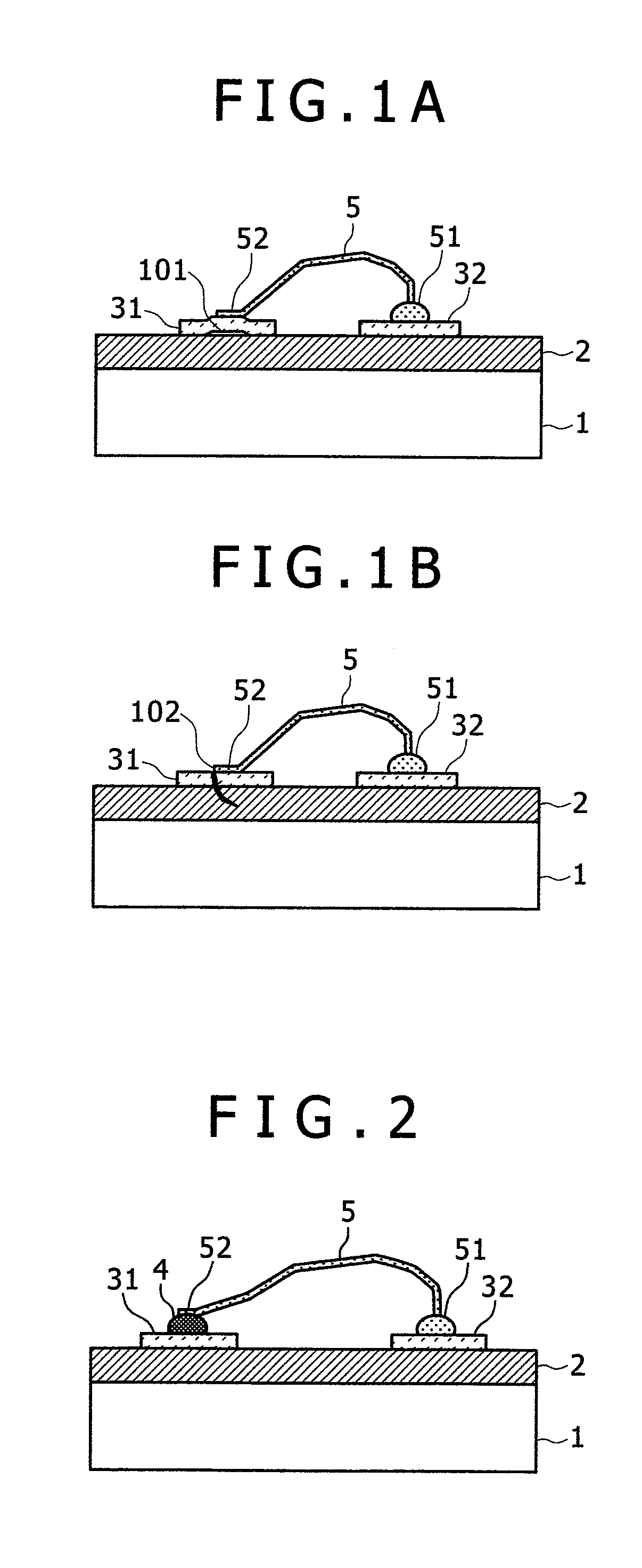
[0026]The description will be made of a first embodiment with reference to FIGS. 2 to 5. Here FIGS. 2 to 5 are cross-sectional views each showing an electronic circuit.
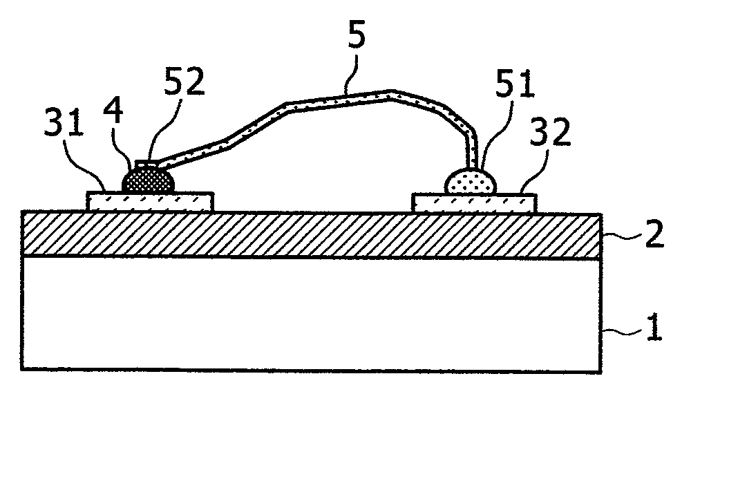
[0027]In FIG. 2, a polyimide film 2 is formed on a surface of a substrate 1. More specifically, polyimide precursor is applied to the substrate 1 by spin coating and then cured (thermally cured) at a temperature of 350° C. Incidentally, the patterning may be performed using photosensitive polyimide before curing, or the patterning may be performed using non-photosensitive polyimide by etching with hydrazine through a photoresist process after curing. An aluminum nitride (AlN) substrate was used as a member of the substrate 1. The film thickness of the polyimide film 2 was 2 μm (after curing). According to the knowledge of the inventors, the maximum effect can be achieved when the film thickness of the insulating resin film is in the range of 0.1 to 100 μm.
[0028]A first bonding pad 31 and second bonding pad 32 of patte...
embodiment 2
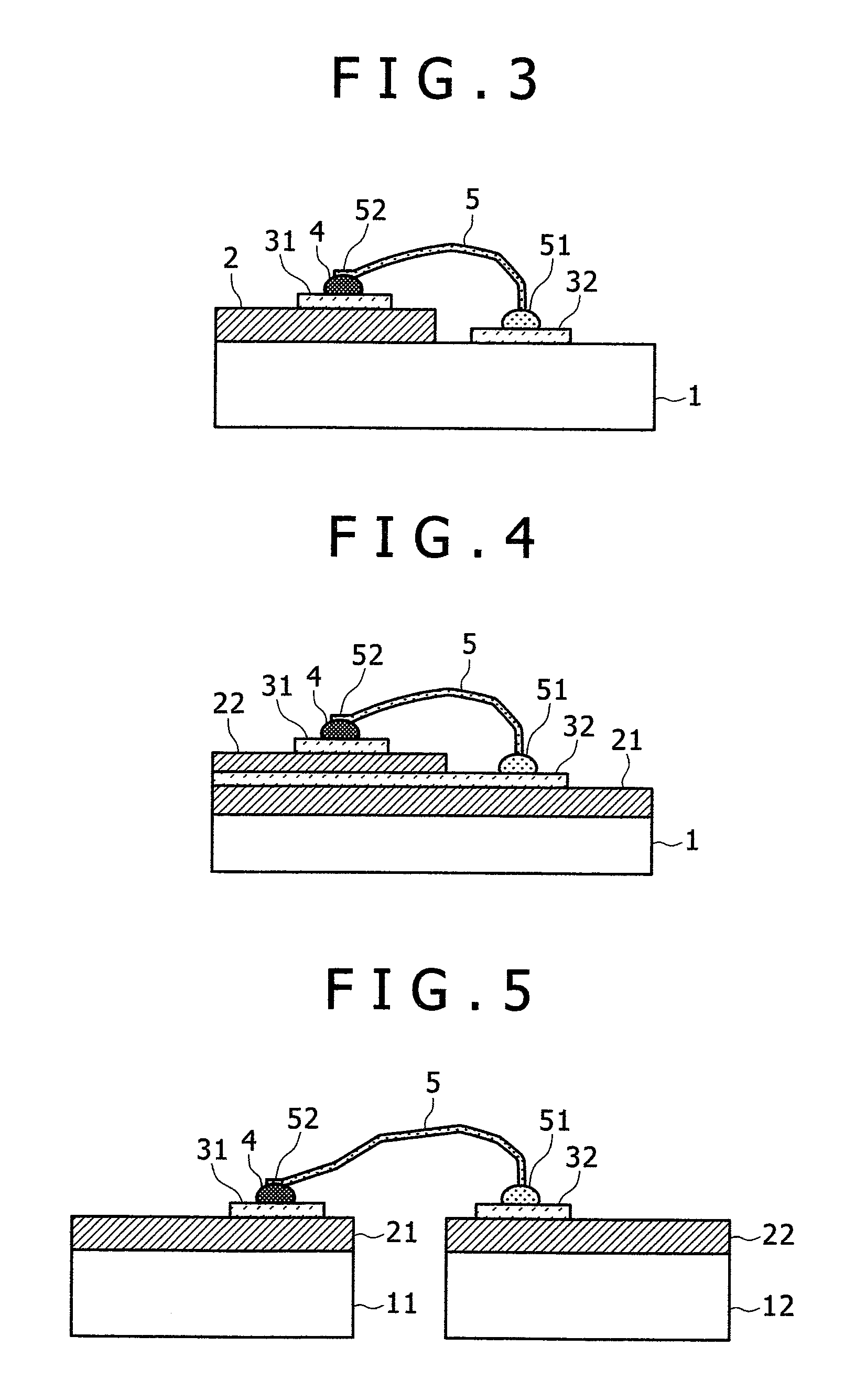
[0041]Next a second embodiment of the present invention will be described with reference to FIGS. 6 and 7. Here FIGS. 6 and 7 are cross-sectional views each showing an electronic circuit.
[0042]First FIG. 6 will be described. In the second embodiment, similarly to the first embodiment, the polyimide film 2 is formed on the surface of the substrate 1. Aluminum nitride was used for the substrate 1, and polyimide was used for the polyimide film 2. The film thickness of polyimide was set to 2 μm.
[0043]The first bonding pad 31 and the second bonding pad 32 are formed on the polyimide film 2. The metallization of the bonding pads 31, 32 is Cr / Al with the film thicknesses of 0.1 / 1.0 μm, respectively.
[0044]Cr / Al was formed sequentially by one sputtering apparatus, without breaking vacuum. Here Cr is a bonding layer, Al is both a wiring layer and a wire bonding layer. The pattern is formed by etching using an aqueous solution of the mixture of phosphoric acid, acetic acid, and nitric acid for...
embodiment 3
[0049]Next, another mode of the present invention will be described as a third embodiment with reference to FIG. 8. Here FIG. 8 includes atop view and a cross-sectional view of an optical module used for optical communication, optical recording, and the like.
[0050]In FIG. 8, a wiring layer 3 of Ti / Pt / Au (thicknesses of 01 / 0.2 / 0.5 μm) is formed on the aluminum nitride substrate 1. The resin insulating layer 2 of polyimide film (thickness of 2 μm) is formed in portion of the upper layer of the wiring layer 3. Further the bonding pad 31 of Ti / Pt / Au (thicknesses of 0.1 / 0.2 / 0.5 μm) is formed on the resin insulating layer 2. The bonding pad 31 also servers as wiring. The bump 4 of Au formed by a ball bonder is provided on the bonding pad 31.
[0051]A semiconductor laser 7 is mounted to portion of the wiring layer 3 on the substrate 1, in which the resin insulating layer 2 is not present, by solder or other suitable means. The semiconductor laser 7 emits light when an electrode 71 in the bot...
PUM
| Property | Measurement | Unit |
|---|---|---|
| Thickness | aaaaa | aaaaa |
| Thickness | aaaaa | aaaaa |
| Electrical conductor | aaaaa | aaaaa |
Abstract
Description
Claims
Application Information