Resurf semiconductor device charge balancing

a semiconductor device and charge balancing technology, applied in semiconductor devices, semiconductor/solid-state device details, electrical devices, etc., can solve problems such as difficulty in consistently achieving volume manufacturing

Active Publication Date: 2009-12-03
NXP USA INC
View PDF18 Cites 69 Cited by
  • Summary
  • Abstract
  • Description
  • Claims
  • Application Information

AI Technical Summary

Problems solved by technology

However, simultaneous optimization of series ON-resistance and breakdown voltage BVdss often requires choices of dop

Method used


Image

  • Resurf semiconductor device charge balancing
  • Resurf semiconductor device charge balancing
  • Resurf semiconductor device charge balancing

Examples


first embodiment

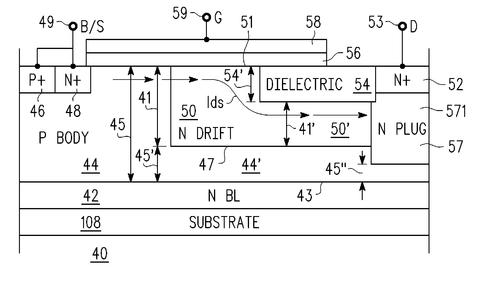
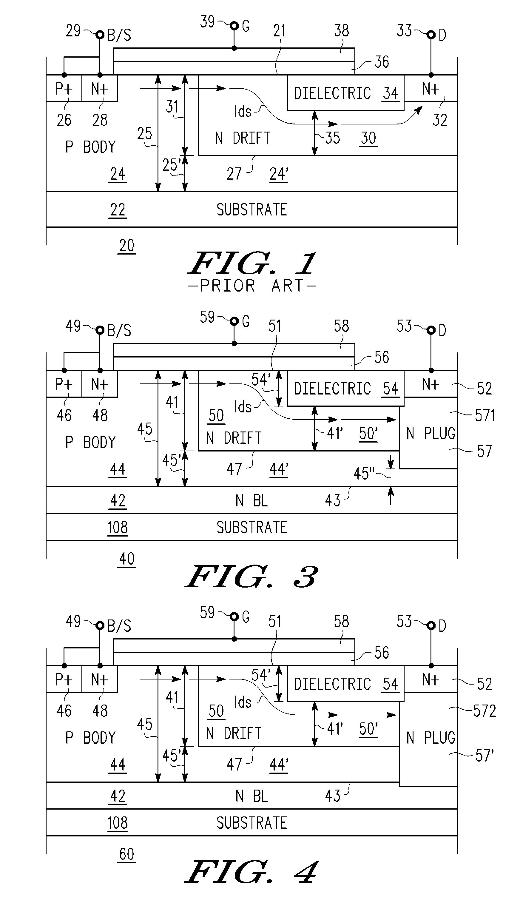
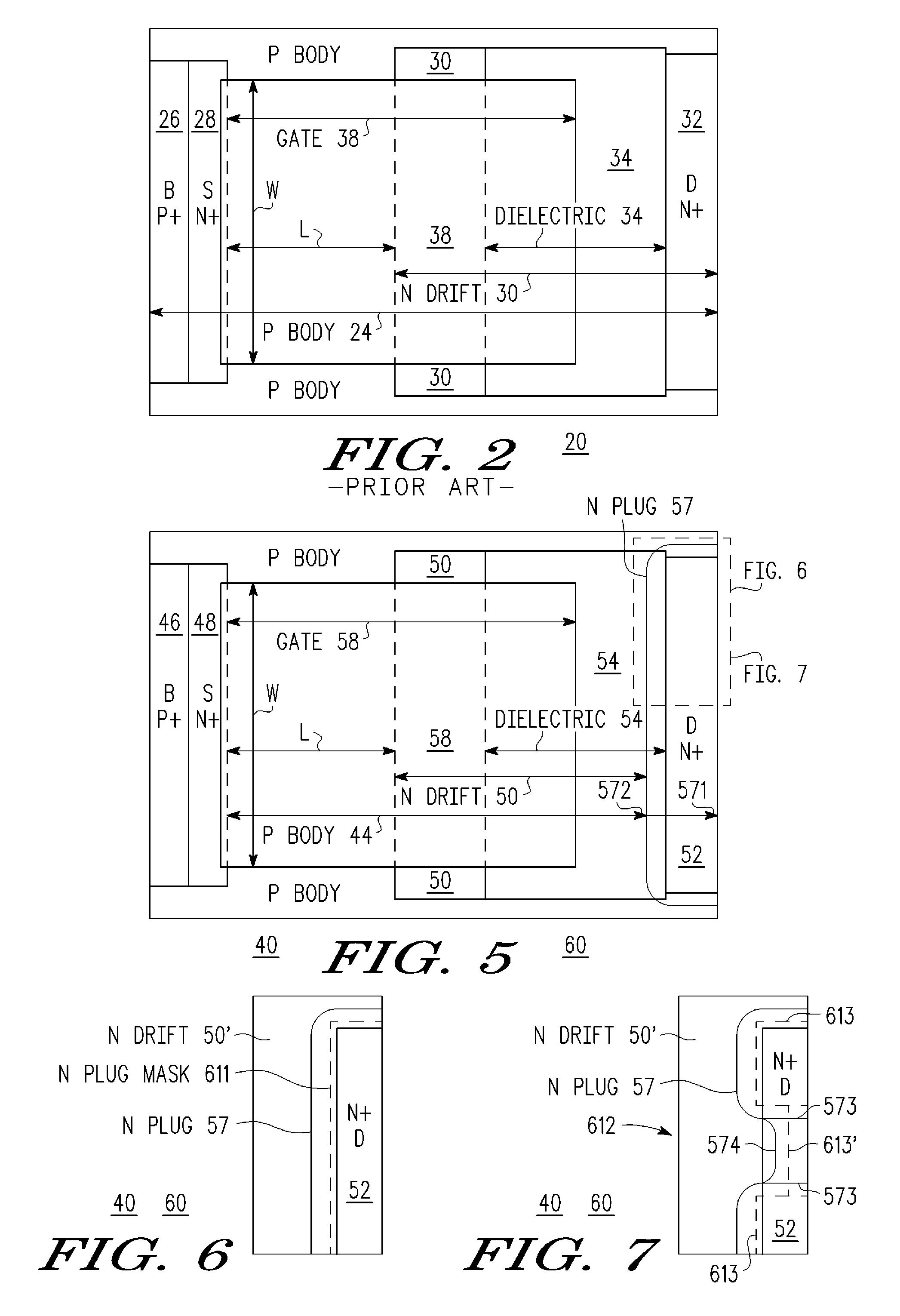
[0043] there is provided a semiconductor device (40, 60, 80, 80′, 80″) employing RESURF charge balancing, comprising, a body region (44, 44′, 84, 84′), a drift region (50, 50′, 90, 90′) located in the body region (44, 44′, 84, 84′), a drain (52, 92) located in the drift region (50, 50′, 90, 90′), a buried layer (42, 82) underlying the body region (44, 44′, 84, 84′), a surrounding doped lateral isolation wall (102) Ohmically coupled to the buried layer (42, 82), wherein RESURF charge balancing is obtained by (i) including a doped sinker (57) coupled to the drain (52, 92) and extending through the drift region (50, 50′, 90, 90′) at least into the underlying body region (44, 44′84, 84′), or (ii) directly or indirectly applying a bias voltage to the buried layer (42, 82), or (iii) a combination of (i) and (ii) above. According to a further embodiment, the device (40, 60, 80, 80′, 80″) further comprises a conductive bridge (104) coupling the drift region (50, 50′, 90, 90′) and the isolat...

second embodiment

[0044] there is provided a method for balancing charge in regions of a RESURF device (40, 60, 80, 80′, 80″), comprising, providing a body region (44, 44′; 84, 84′) of a first conductivity type, having a portion (44, 84) extending to a first surface (51, 91) and to a first depth (45, 85) from the first surface (51, 91), providing a source region (48, 88) of a second opposite conductivity type in the body region (44, 44′; 84, 84′) proximate the first surface (51, 91), providing a drift region (50, 50′, 90, 90′) of a second opposite conductivity type in the body region (44, 44′; 84, 84′) spaced apart from the source region (48, 88) and having a portion (50, 90) extending to the first surface (51, 91) and to a second depth (41, 81) less than the first depth (45, 85), providing a drain region (52, 92) of the second opposite conductivity type in the drift region (50, 50, 90, 90′), spaced apart from the body region (44, 44′, 84, 84′) and proximate the first surface (51, 91), and providing ...

third embodiment

[0045] there is provided a method for controlling charge balancing in a RESURF device (40, 60, 80, 80′, 80″) having a source (48, 88) of a first conductivity type, a drift region (50, 50′, 90, 90′) of the first conductivity type, a drain region (52, 92) of the first conductivity type within the drift region (50, 50, 90, 90′), a body region (44, 44′, 84, 84′) of a second, opposite, conductivity type having a first portion (44, 84) between the source (48, 88) and the drift region (50, 50′, 90, 90′) and a second portion (44′, 84′) underlying the drift region (50, 50′, 90, 90′) and a buried layer region (42, 82) of the first conductivity type underlying the body region (44, 44′, 88, 88′), the method comprising, forming an isolation wall (102) laterally surrounding the device (40, 60, 80, 80′, 80″) that is Ohmically coupled to the buried layer region (42, 82), forming a variable resistance bridge (104) between the isolation wall (102) and the drift region (50, 50′, 90, 90′), and transmit...


PUM


Abstract

Breakdown voltage BVdss is enhanced and ON-resistance reduced in RESURF devices (40, 60, 80, 80′, 80″), e.g., LDMOS transistors, by careful charge balancing, even when body (44, 44′, 84, 84′) and drift (50, 50′, 90, 90′) region charge balance is not ideal, by: (i) providing a plug or sinker (57) near the drain (52, 92) and of the same conductivity type extending through the drift region (50, 50′, 90, 90′) at least into the underlying body region (44, 44′ 84, 84′), and/or (ii) applying bias Viso to a surrounding lateral doped isolation wall (102) coupled to the device buried layer (42, 82), and/or (iii) providing a variable resistance bridge (104) between the isolation wall (102) and the drift region (50, 50′, 90, 90′). The bridge (104) may be a FET (110) whose source-drain (113, 114) couple the isolation wall (102) and drift region (50, 50′, 90, 90′) and whose gate (116) receives control voltage Vc, or a resistor (120) whose cross-section (X, Y, Z) affects its resistance and pinch-off, to set the percentage of drain voltage coupled to the buried layer (42, 82) via the isolation wall (102).

Description

FIELD OF THE INVENTION[0001]The present invention generally relates to reduced surface field (RESURF) means and methods for semiconductor devices and, more particularly, means and methods for charge balancing in RESURF semiconductor devices.BACKGROUND OF THE INVENTION[0002]It is known that reduced surface field (RESURF) techniques can be applied to various semiconductor devices to improve their voltage breakdown and their series ON-resistance. However, simultaneous optimization of series ON-resistance and breakdown voltage BVdss often requires choices of doping and device geometry that may be unduly restrictive and difficult to achieve consistently in volume manufacturing. Accordingly, there is an on-going need for improved RESURF structures and methods that allow greater flexibility in device design and the charge balancing needed for RESURF behavior.[0003]For convenience of explanation, the improvements described herein are illustrated by means of lateral diffused field effect MOS...

Claims


Application Information

Patent Timeline
IPC IPC(8): H01L29/78H01L23/58
CPCH01L29/0847H01L29/7835H01L29/1087H01L29/0653H01L29/1083H01L29/7816H01L29/0692H01L2924/0002H01L29/063H01L29/0634H01L2924/00H01L29/0882H01L29/1095H01L29/7823
Inventor MIN, WON GIZHANG, ZHIHONGXU, HONGZHONGZUO, JIANG-KAI
Owner NXP USA INC
Why Eureka
Try Eureka