Semiconductor memory device

a memory device and semiconductor technology, applied in the field of semiconductor memory devices, can solve the problems of erroneous read, erase cell is not detected, and the drain-source voltage of the memory cell is difficult to control

Inactive Publication Date: 2009-12-10
KK TOSHIBA
View PDF16 Cites 7 Cited by
  • Summary
  • Abstract
  • Description
  • Claims
  • Application Information

AI Technical Summary

Benefits of technology

[0019]the select gate transistor is NMOS transistor, and the select gate line driver is configured to drive the NMOS transistor so as to clamp the source voltage at a substantially constant level independently of the bit line resistance at a read time.

Problems solved by technology

In a NAND-type flash memory, in which size-shrinking, integration and capacitance increase are progressing, the bit line becomes highly resistive, and it leads to difficulty of controlling the drain-source voltage of the memory cell due to the voltage drop of the bit line resistance.
Therefore, even if an erase cell is set in a sufficiently low threshold voltage state, there is a possibility of generating an erroneous read such that the erase cell is not detected as it is.

Method used


Image

  • Semiconductor memory device
  • Semiconductor memory device
  • Semiconductor memory device

Examples


Embodiment Construction

[0034]Illustrative embodiments of this invention will be explained with reference to the accompanying drawings below.

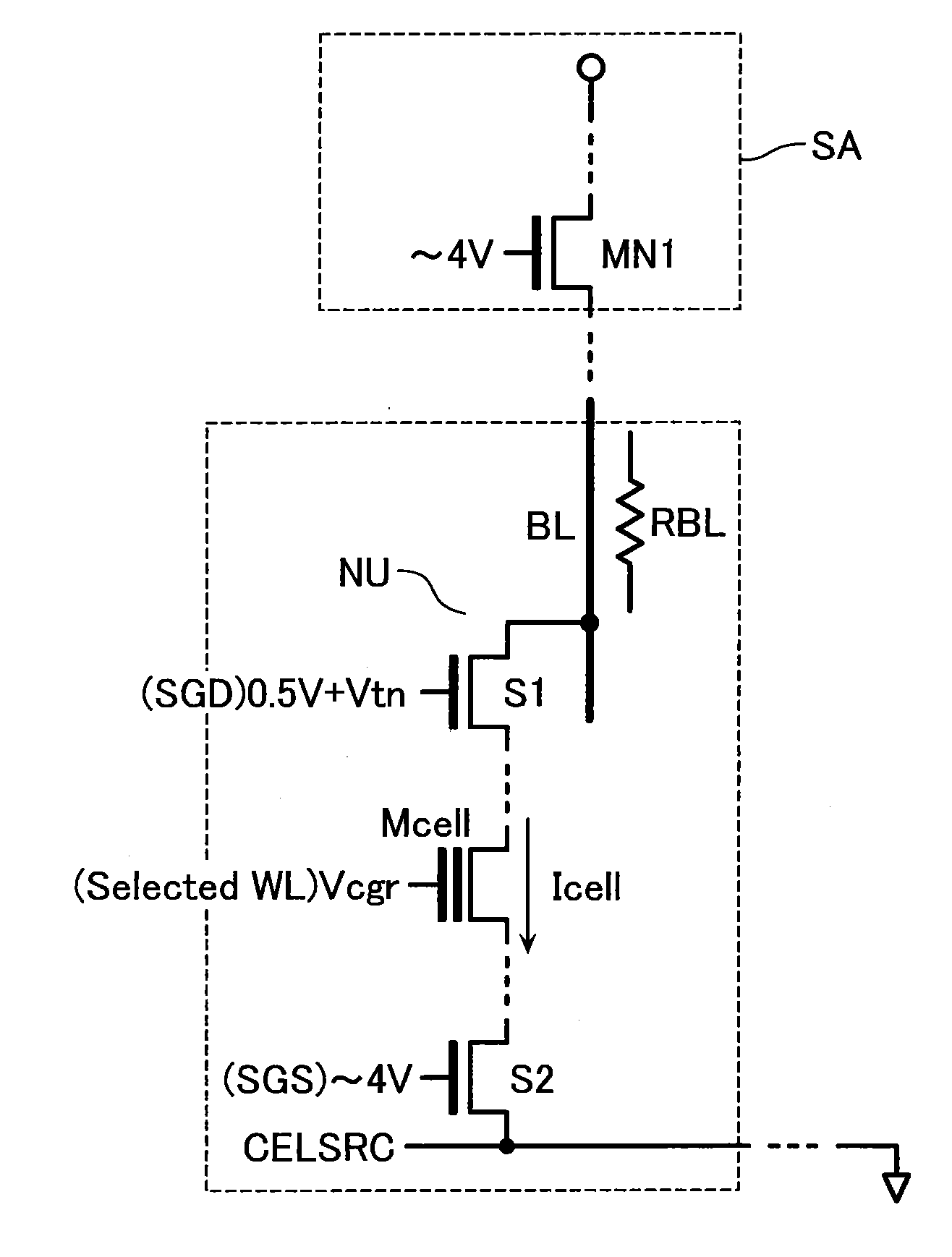
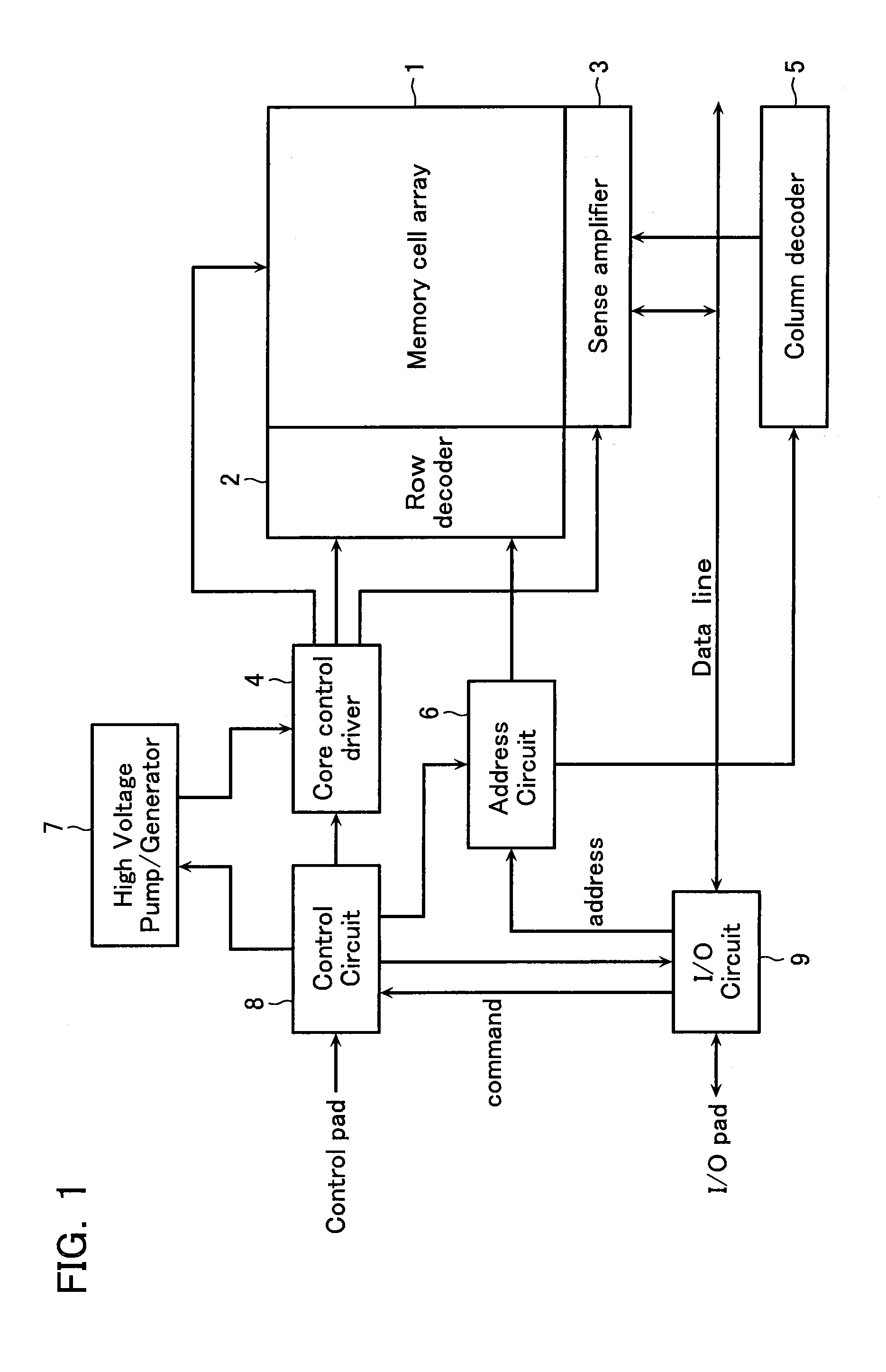
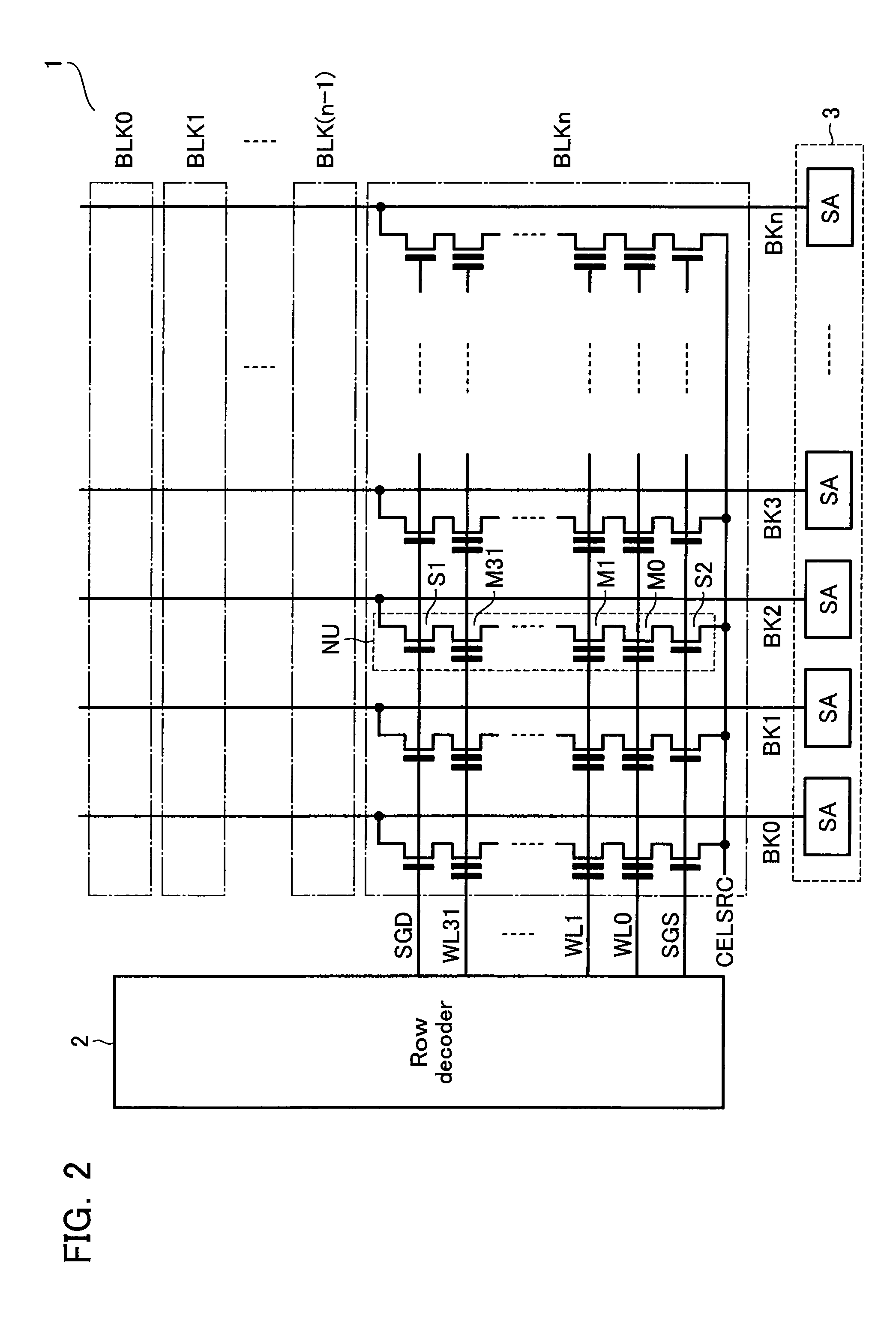
[0035]FIG. 1 shows a functional block configuration of a NAND-type flash memory in accordance with an embodiment, and FIG. 2 shows the memory core. Memory cell array 1 is, as shown in FIG. 2, formed of NAND cell units (NAND strings), NU, arranged therein, each of which has multiple memory cells M0-M31 connected in series.

[0036]The memory cell has a MOS transistor structure, in which a floating gate and a control gate are stacked, and stores data defined by a high threshold state obtained by injecting electrons into the floating gate and a low threshold state obtained by discharging electrons stored in the floating gate. Alternatively, it may be used another cell structure, in which a charge trap layer or boundary is formed in the gate insulating film, and the same data storage is done as that of the above-described floating gate type of memory cell.

[0037]One end of th...


PUM


Abstract

A semiconductor memory device including: a memory cell coupled to a bit line via a select gate transistor; a sense amplifier configured to have a current source for supplying current to the bit line, and detect cell current of the memory cell flowing on the bit line; and a select gate line driver configured to drive the select gate transistor so as to keep the memory cell applied with substantially constant drain-source voltage independently of the bit line resistance at a read time.

Description

CROSS-REFERENCE TO RELATED APPLICATION[0001]This application is based on and claims the benefit of priority from the prior Japanese Patent Application No. 2008-146611, filed on Jun. 4, 2008, the entire contents of which are incorporated herein by reference.BACKGROUND OF THE INVENTION[0002]1. Field of the Invention[0003]This invention relates to a semiconductor memory device, specifically to a sense scheme of a highly integrated memory device.[0004]2. Description of the Related Art[0005]A NAND-type flash memory is well known as one of electrically rewritable and non-volatile semiconductor memories (EEPROMs). As a sense amplifier used in the NAND-type flash memory, it is known such a current-sensing type of sense amplifier as to detect cell current of a selected memory cell under the condition that the selected memory cell is applied with drain-source voltage of about 0.5V (refer to, for example, JP-A-2006-500727). In this sense scheme, the drain-source voltage of the selected memory ...

Claims


Application Information

Patent Timeline
Patent Type & Authority Applications(United States)
IPC IPC(8): G11C16/04G11C16/06G11C7/10
CPCG11C7/06G11C16/0483G11C2207/068G11C16/28G11C16/30G11C16/08
Inventor ABE, TAKUMI
Owner KK TOSHIBA
Why Eureka
Try Eureka