Isolation Trenches with Conductive Plates

a technology of conductive plates and isolation trenches, which is applied in the direction of semiconductor devices, electrical equipment, transistors, etc., can solve the problems of reducing the size of the device, the isolation region may not be sufficient to provide isolation for adjacent active areas or devices, and the leakage current and parasitic effects between adjacent devices

Inactive Publication Date: 2009-12-24
POLARIS INNOVATIONS
View PDF6 Cites 71 Cited by
  • Summary
  • Abstract
  • Description
  • Claims
  • Application Information

AI Technical Summary

Benefits of technology

This patent provides new ways to create isolated areas on semiconductor devices. These techniques involve adding an extra layer called a conductive plate at the bottom of the holes where these regions will be formed. This helps improve the performance of the device by making it more efficient with its electricity distribution.

Problems solved by technology

The technical problem addressed in this patent text is how to improve the formation of isolation regions in semiconductor devices to better prevent leaks and minimize interference between neighboring active areas.

Method used


Image

  • Isolation Trenches with Conductive Plates
  • Isolation Trenches with Conductive Plates
  • Isolation Trenches with Conductive Plates

Examples


Embodiment Construction

[0021]The making and using of the presently preferred embodiments are discussed in detail below. It should be appreciated, however, that the present invention provides many applicable inventive concepts that can be embodied in a wide variety of specific contexts. The specific embodiments discussed are merely illustrative of specific ways to make and use the invention, and do not limit the scope of the invention.

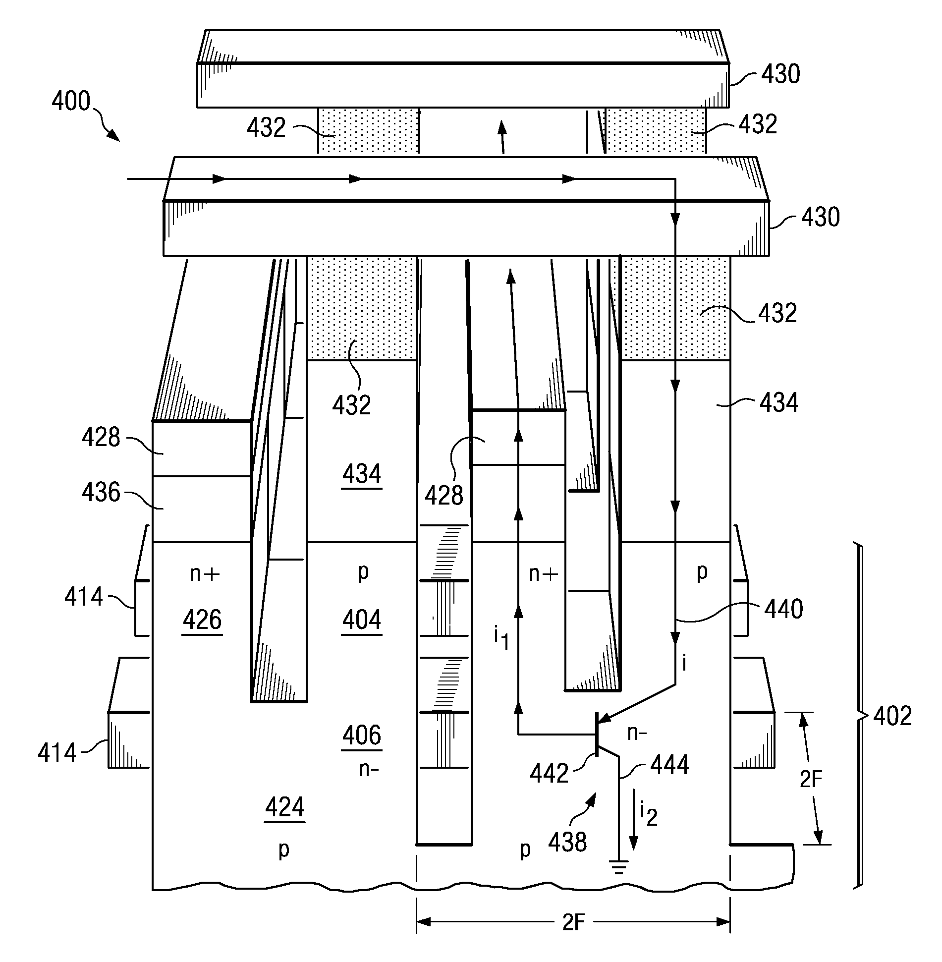
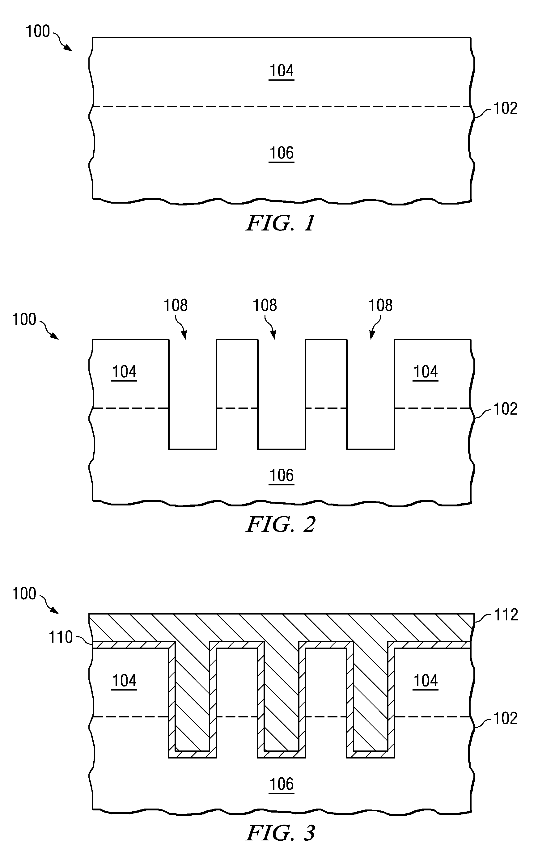
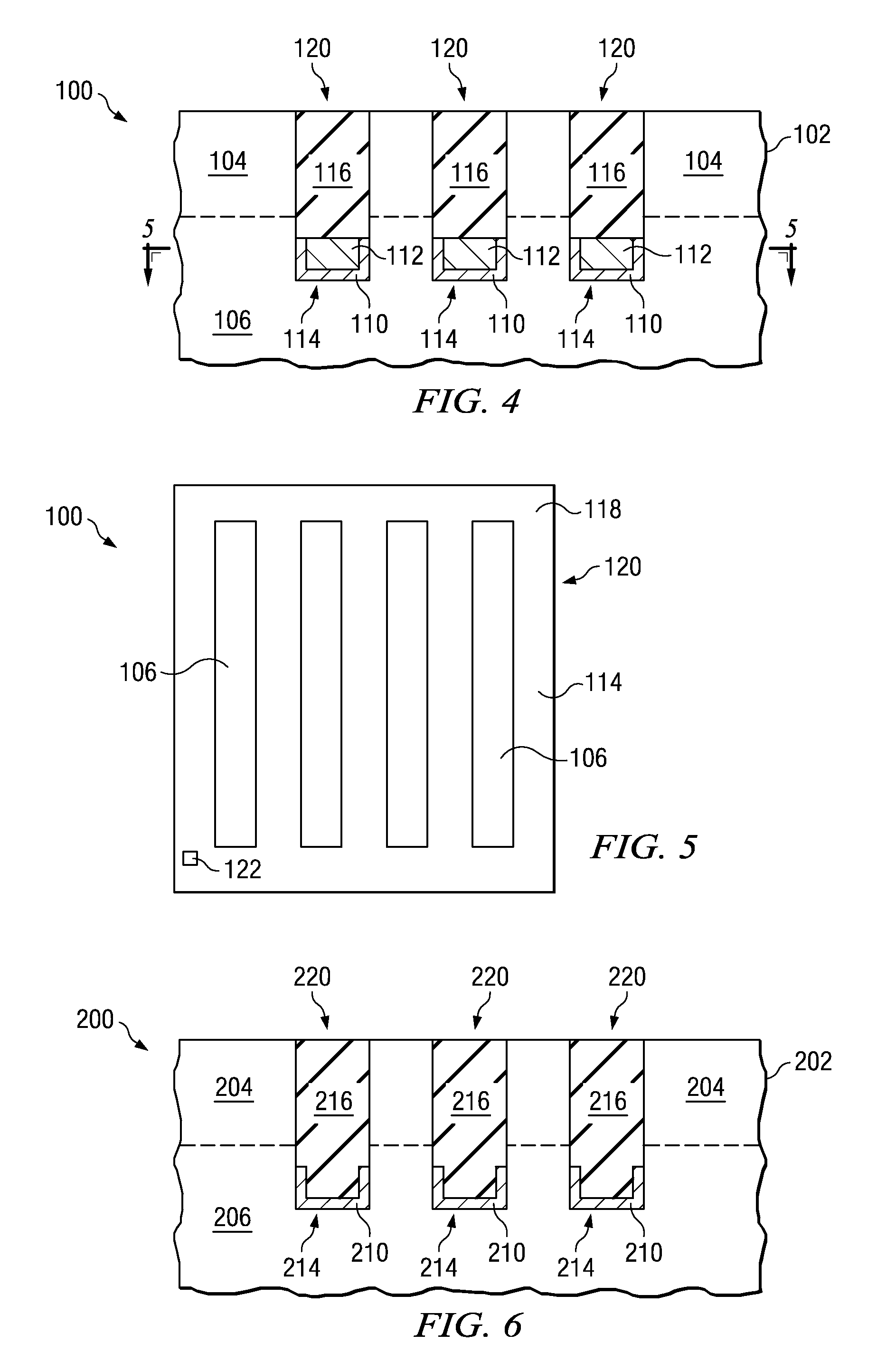
[0022]There is a trend in semiconductor technology to reduce the size of devices, to improve performance and reduce power requirements, as examples. The minimum feature size or critical dimension (CD) of semiconductor devices continues to become smaller and smaller. For example, advanced technology nodes are developing 60 nm, 45 nm, and 32 nm CDs, and the trend in reducing CD's is expected to continue towards the 20 nm or less range.

[0023]Some features of semiconductor devices may comprise the minimum feature size or CD of a technology node, such as isolation regions, bitline...


PUM


Abstract

Methods of forming isolation trenches, semiconductor devices, structures thereof, and methods of operating memory arrays are disclosed. In one embodiment, an isolation trench includes a recess disposed in a workpiece. A conductive material is disposed in a lower portion of the channel. An insulating material is disposed in an upper portion of the recess over the conductive material.

Description


Claims


Application Information

Patent Timeline
Owner POLARIS INNOVATIONS
Why Eureka
Try Eureka