Electro-optical device and method of driving the same

a technology of optical devices and optical components, applied in the direction of optics, static indicating devices, instruments, etc., can solve problems such as extreme difficulty

Inactive Publication Date: 2005-03-10
SEMICON ENERGY LAB CO LTD
View PDF55 Cites 32 Cited by
  • Summary
  • Abstract
  • Description
  • Claims
  • Application Information

AI Technical Summary

Benefits of technology

[0010] An object of the present invention is to propose a completely novel method of gradation display which has been conventionally difficult. According to the present invention, an intermediate gradation display is carried out not by applying an analog signal as has been in a prior art, but by applying a digital signal, and by means of the duration of the application. For this purpose, an analog image signal is digitized through binary system calculation, and is stored in a memory device, and the data is retrieved, calculated, and is outputted to a display device (an electro-optical device), as required. As a result of this, an advanced gradation of no less than 16 gradations is achieved, which has been extremely difficult by the prior art of analog gradation display method.

Problems solved by technology

As a result of this, an advanced gradation of no less than 16 gradations is achieved, which has been extremely difficult by the prior art of analog gradation display method.

Method used


Image

  • Electro-optical device and method of driving the same
  • Electro-optical device and method of driving the same
  • Electro-optical device and method of driving the same

Examples


embodiment 1

[0078] Preferred Embodiment 1

[0079] In this embodiment, a wall mounted television set was manufactured by using the liquid crystal device utilizing the circuit structure as shown in FIG. 5, which will be described infra. Polycrystalline silicon that received laser annealing was used for TFT at the time of manufacturing.

[0080] The actual arrangement or structure of electrodes etc. corresponding to this circuit structure is shown in FIG. 6, for one picture element. The manufacturing method of the liquid crystal panel used in the first preferred embodiment will be first explained with reference to FIGS. 7 and 8. FIGS. 7 and 8 are cross sectional views and plan views of the liquid crystal panel, respectively. Referring to FIG. 7(A), a silicon oxide film was manufactured at a thickness of 1000-3000 angstroms as a blocking layer 51 by magnetron RF (high frequency) sputtering, on a glass substrate 50, which is not expensive such as quartz, and which can bear the thermal treatment of no mo...

embodiment 2

[0106] Preferred Embodiment 2

[0107] In this embodiment, a wall mounted television set manufactured by using a liquid crystal display device having a circuit structure as shown in FIG. 5, will be explained. Polycrystalline silicon subjected to laser annealing was used for TFT.

[0108] The manufacturing of a TFT part will be described infra according to FIG. 9. Referring to FIG. 9(A), a silicon oxide film was manufactured as a blocking layer 101 on an inexpensive glass substrate 100 which bears the heat treatment of not more than 700° C., e.g. approximately 600° C., at a thickness of 1000-3000 angstroms by magnetron RF (high frequency) sputtering. The conditions for the process were: in 100% oxygen atmosphere; the temperature for film formation was 15° C.; output was 400-800 W; and, pressure was 0.5 Pa. The rate of film formation was 30-100 angstroms / min, when quartz or single crystalline silicon was used as a target.

[0109] A silicon film 102 was manufactured thereon by plasma CVD. Th...

embodiment 3

[0124] Preferred Embodiment 3

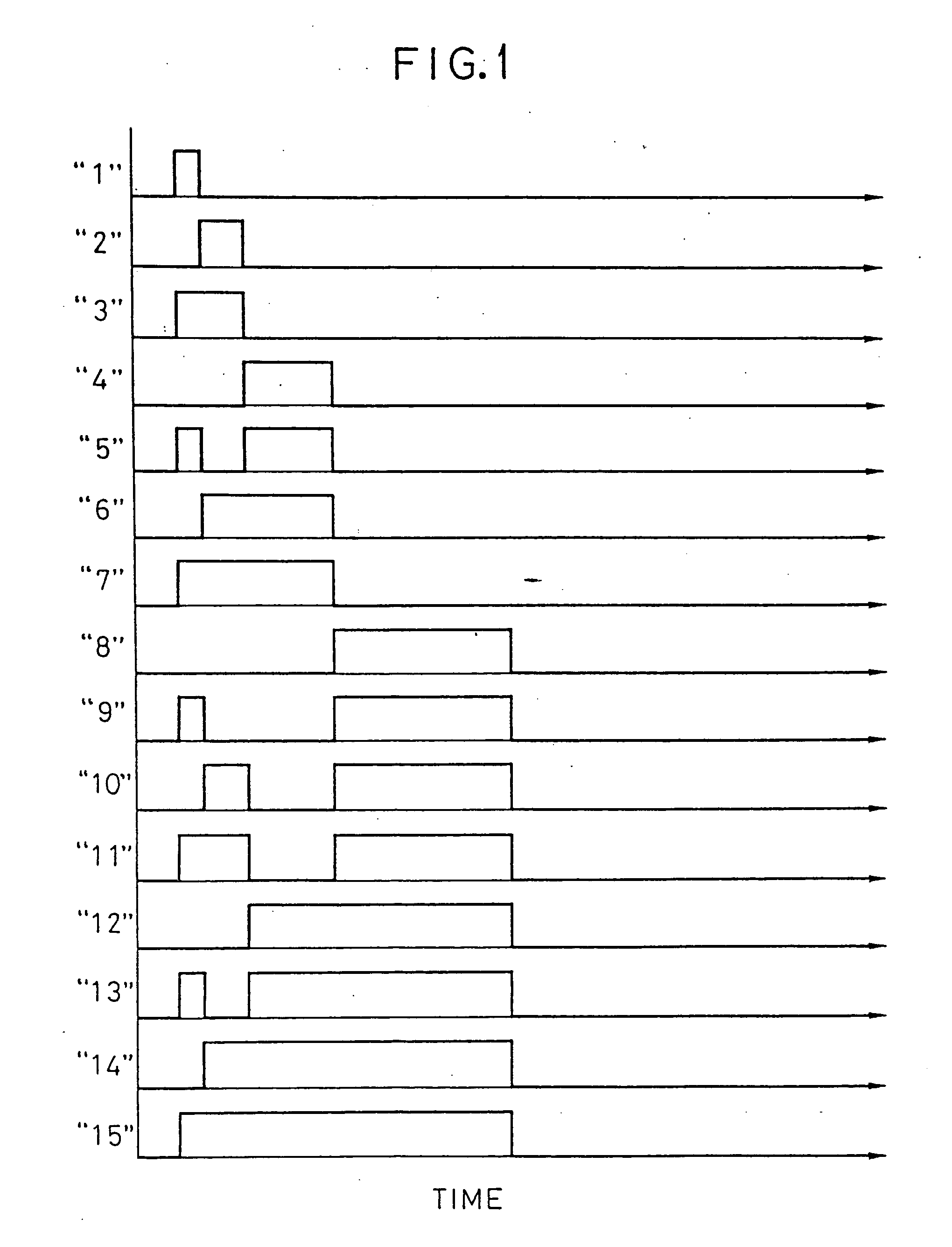
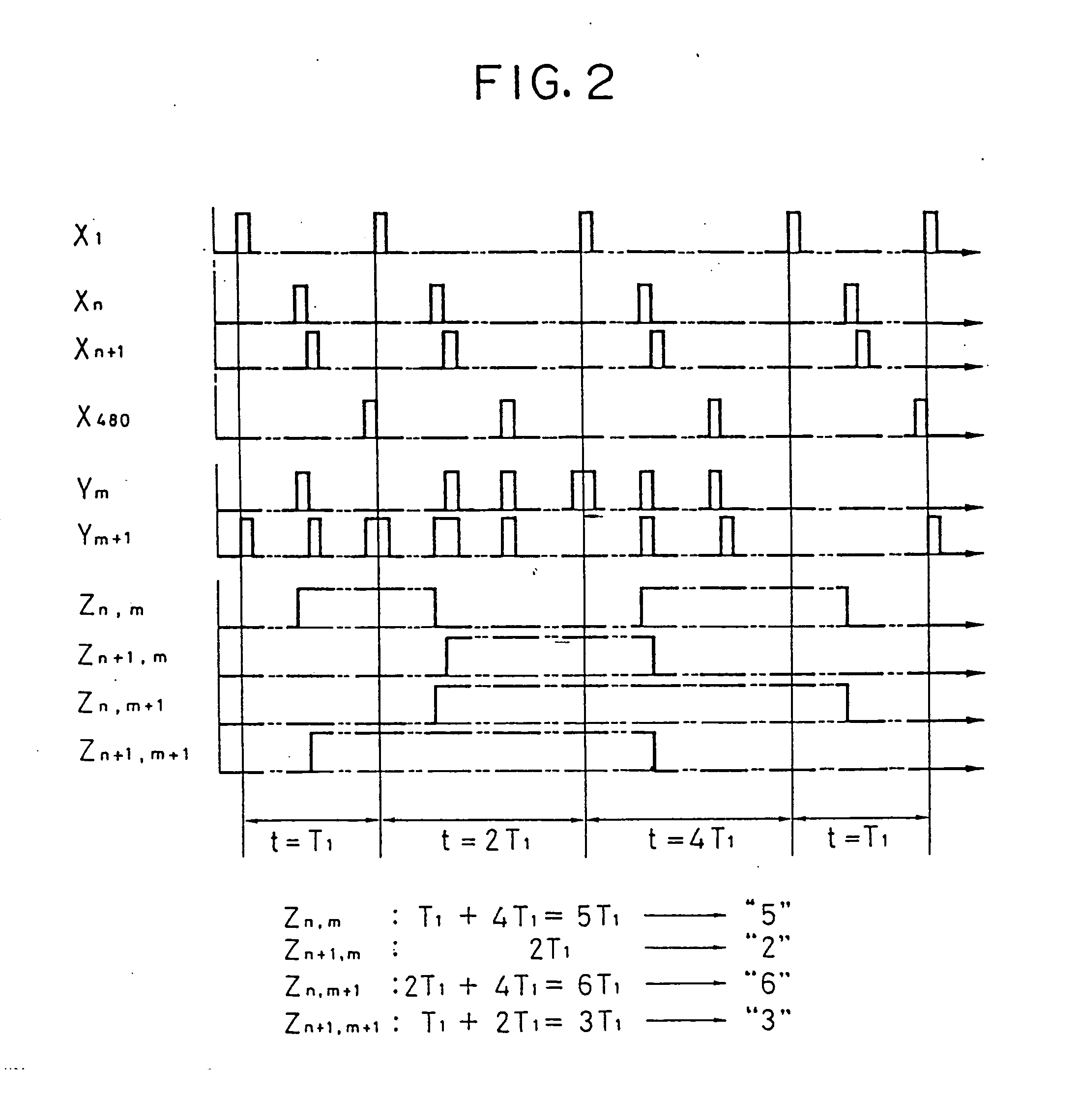
[0125] A device used when an actual monochrome television (NTSC) was driven in accordance with the present invention, is shown in FIGS. 20, 21 and 23, and examples of driving signals are shown in FIGS. 22 and 24.

[0126] A screen of the television and a peripheral circuit thereof are shown in FIG. 20, and the size of the matrix of the screen is 720×480. FIFO is thus of 720×480×3=1036800 bits, and a driver and a shift register of X-line are of 480 dots, while those of Y-line are of 720 dots. A data shift register of Y-line was of 16 bits×45. The timings of these were controlled by a sequence controller of gradation driving of LCD.

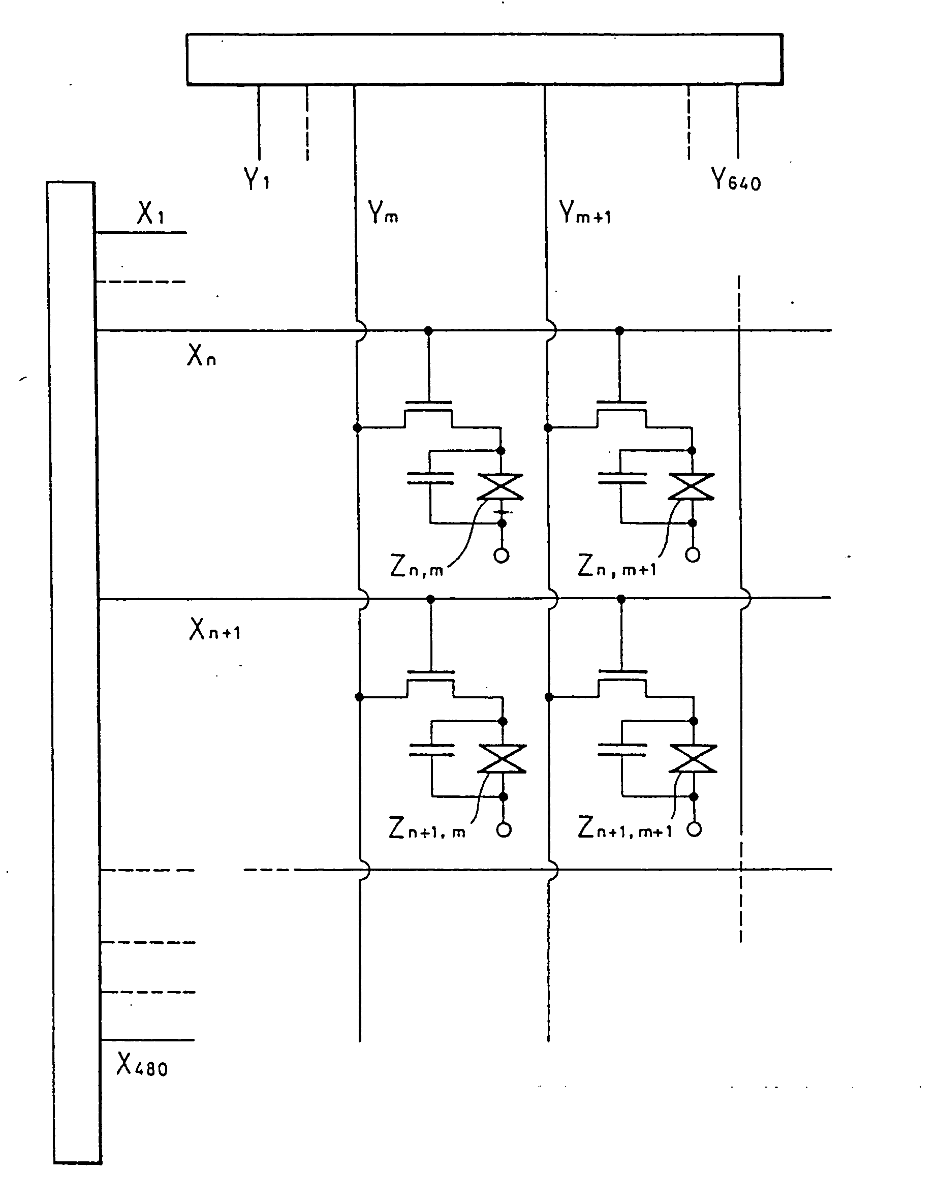
[0127] A polysilicon TFT CMOS (complementary field effect device) transfer gate circuit was used to form a matrix of the screen. The schematic circuit diagram related to the four picture elements is shown in FIG. 23. At the time of manufacturing, a normal low temperature thermal annealing crystallization method was adopted. The d...


PUM

PropertyMeasurementUnit
response timeaaaaaaaaaa
voltageaaaaaaaaaa

Abstract

The method of fine gradation display by an electro-optical device with little influence by difference in elemental devices, is disclosed, which is an object of the present invention. In case of an active matrix electro-optical device, a visual gradation display can be carried out by digitizing an analog image signal externally supplied by means of binary notation, by temporarily storing the digital signal thus obtained, by outputting the digital signal to a circuit of next step in a proper order, and by controlling the output timing of the signal so as to output the signal to the active matrix electro-optical device, and whereby digitally controlling the time for applying voltage to a picture element.

Description

BACKGROUND OF THE INVENTION [0001] 1. Field of the Invention [0002] The present invention relates to an electro-optical device and a method of driving the same, and, in particular, to the method of gradation image display for obtaining the expression having neutral color tone or intermediate brightness, by utilizing a thin film transistor (hereinafter referred to as TFT) as a switching device for driving. The present invention relates, in particular, to the complete digital gradation display for performing a gradation display without applying any external analog signal to an active device. [0003] 2. Description of the Prior Art [0004] A liquid crystal composition can easily be oriented in a parallel direction or in a vertical direction to an external electric field existing outside thereof, because the dielectric constant of the liquid crystal composition in a direction parallel to the molecule axis thereof is different from that in a direction vertical to the molecule axis. The ON / ...

Claims


Application Information

Patent Timeline
Patent Type & Authority Applications(United States)
IPC IPC(8): G02F1/1362G09G3/20G09G3/36G09G5/395
CPCG02F1/136227G09G3/2018G09G3/3648G09G3/3677G09G2330/04G09G3/3688G09G5/395G09G2300/0823G09G2310/027G09G3/3685
Inventor YAMAZAKI, SHUNPEIMASE, AKIRAHIROKI, MASAAKI
Owner SEMICON ENERGY LAB CO LTD
Why Eureka
Try Eureka