MEMS Stiction Testing Apparatus and Method

a technology of stiction testing and mems, which is applied in the direction of microstructural devices, instruments, and mechanical means, can solve the problems of stiction problems, many currently available stiction tests of mems devices, and inoperable devices, and achieve the effect of mitigate the first electrical signal and low valu

Active Publication Date: 2009-12-31
ANALOG DEVICES INC
View PDF18 Cites 29 Cited by
  • Summary
  • Abstract
  • Description
  • Claims
  • Application Information

AI Technical Summary

Benefits of technology

[0007]To substantially mitigate the first electrical signal, the method may completely turn off the first electrical signal, or reduce it to a very low value. Moreover, the method may monitor the second electrical signal to determine when the first electrical signal should be mitigated.

Problems solved by technology

Undesirably, extremely clean microstructure surfaces often stick together if they come into contact.
When the surfaces remain stuck together, the device often is inoperable.
Many currently available MEMS device stiction tests, however, have significant limitations.
For example, some known stiction tests (which, of course, are not used during actual use of the MEMS device) in fact cause the stiction problem.
Consequently, in addition to destroying the MEMS device, such tests do not accurately determine if a stiction problem actually exists.
Other tests are not usable with certain types of MEMS devices.
For example, some stiction tests are not usable with MEMS devices having springs with a high spring constant.

Method used


Image

  • MEMS Stiction Testing Apparatus and Method
  • MEMS Stiction Testing Apparatus and Method
  • MEMS Stiction Testing Apparatus and Method

Examples


example 1

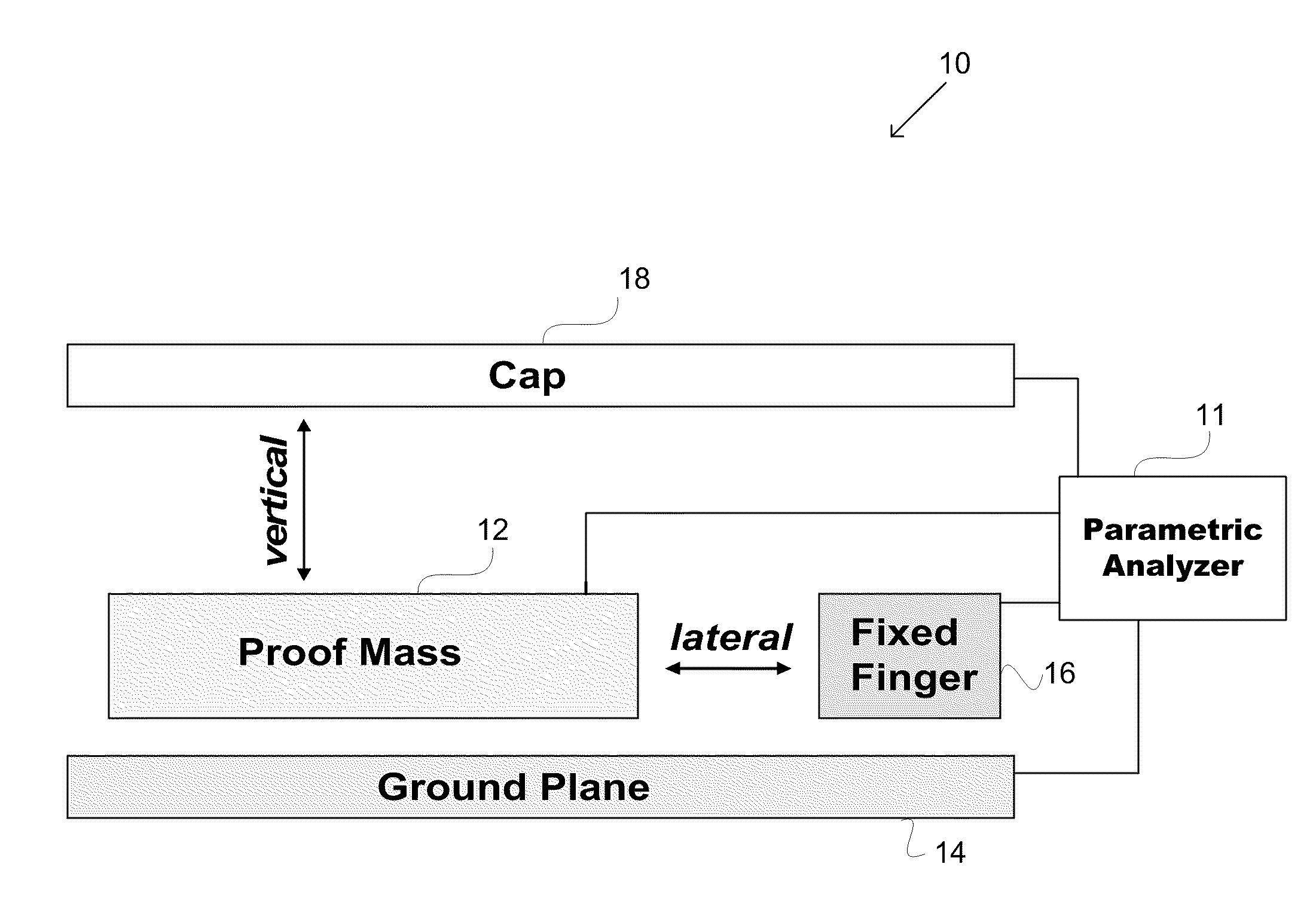
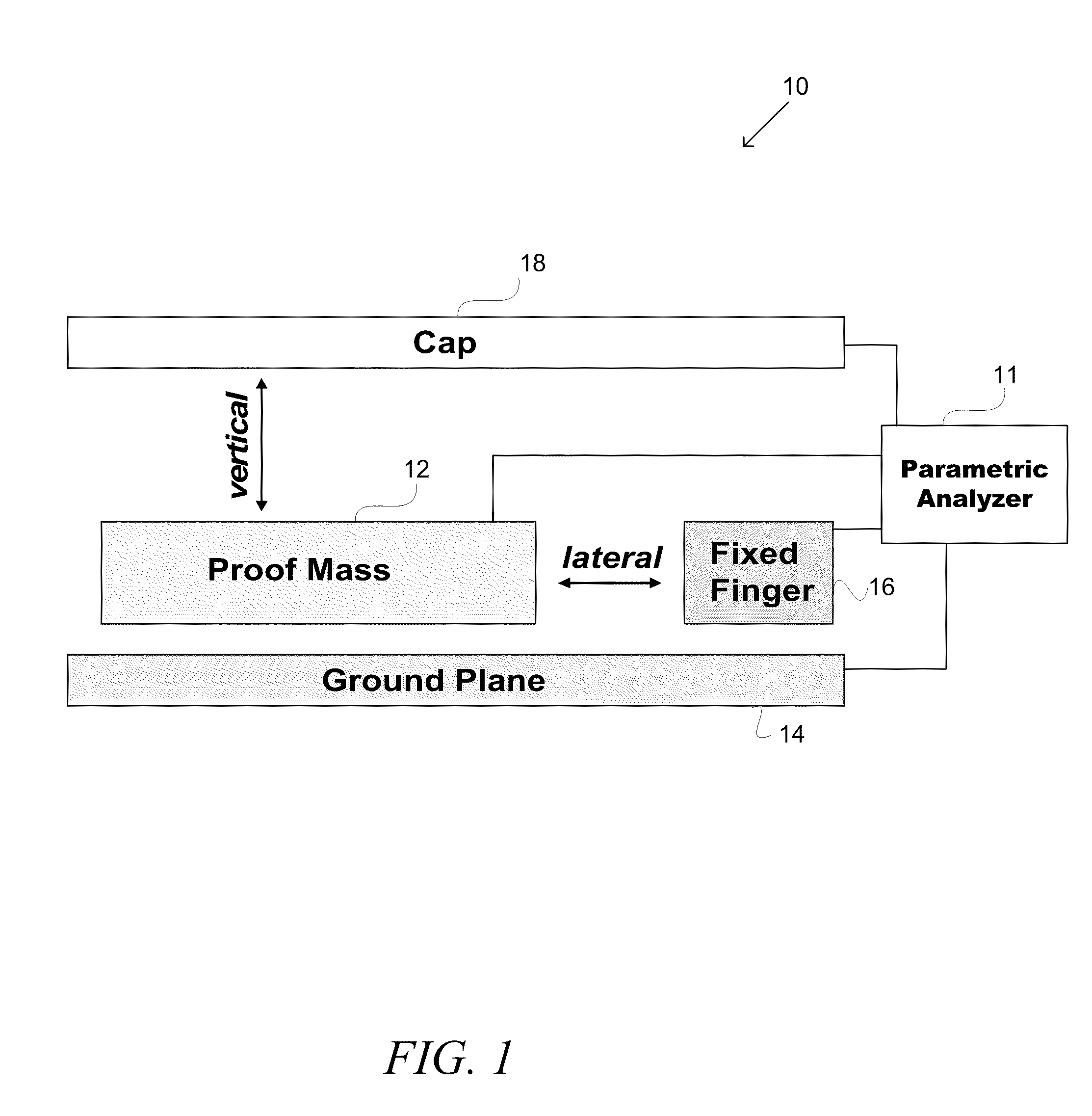
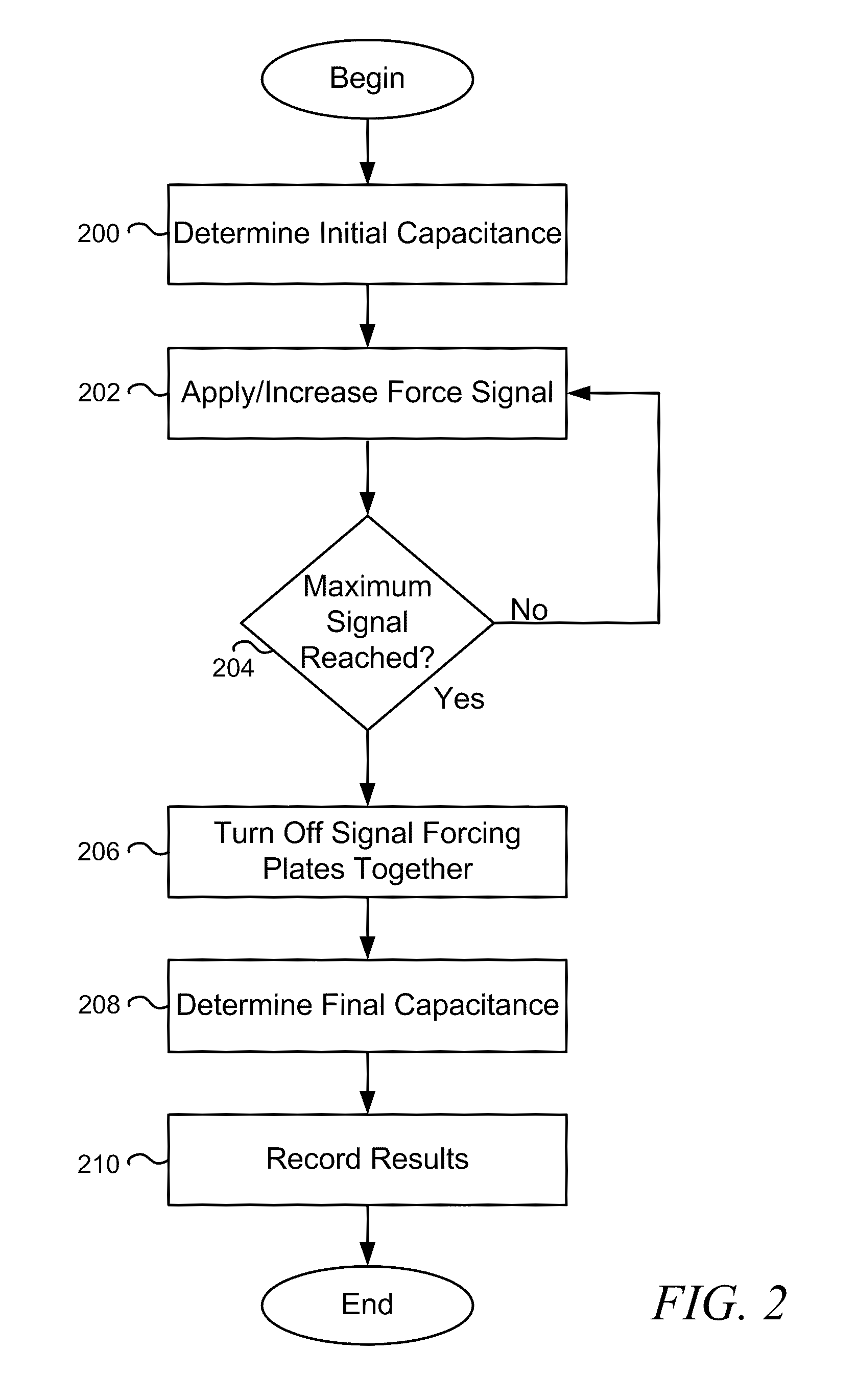
[0055]If current is detected when determining the initial capacitance (e.g., at step 200 in FIG. 2) or at the lowest test voltage (e.g., at step 202 in FIG. 2), then the two surfaces already may be in contact with one another (e.g., due to stiction, fabrication defect, or breakage) or another failure condition may exist (e.g., a short circuit). The logic flow of FIG. 2 could be modified to proceed directly to block 210 if such a condition exists.

example 2

[0056]If a predetermined maximum test voltage (force) is reached without detecting the maximum current, then the movable part may be stuck or impeded (e.g., due to stiction elsewhere, incomplete release of the movable part, springs that are too stiff, or other defect or impediment). The logic flow of FIG. 2 could be modified to terminate the loop between blocks 202 and 204 and proceed to block 210 if a maximum force signal is reached without detecting contact between the test surfaces.

example 3

[0057]Even if a MEMS device passes the stiction test (i.e., the surfaces are forced together and then separate properly), the MEMS device still may be considered defective or unsuitable for a particular purpose. For example, if a larger or smaller than expected test voltage is needed to force the surfaces together (e.g., due to springs that are too stiff or too pliable), the MEMS device may be flagged as being defective or suspect. The logic flow of FIG. 2 could be modified to record an appropriate device status if contact is detected at a force signal that is above or below a predetermined force signal threshold.

[0058]Thus, it should be noted that the process of FIG. 2 is but one of many different processes that can implement illustrative embodiments of the invention. For example, some processes affirmatively measure and record the pullout voltage. Such processes often use this pullout voltage (which is a function of stiction) to further optimize the MEMS fabrication process. Such ...


PUM

PropertyMeasurementUnit
voltageaaaaaaaaaa
voltageaaaaaaaaaa
voltageaaaaaaaaaa

Abstract

A MEMS stiction testing method applies a first electrical signal to a MEMS device having two opposing surfaces to cause the two opposing surfaces to make physical contact. The two opposing surfaces produce a second electrical signal when in physical contact. The method then substantially mitigates the first electrical signal after detecting that the second electrical signal has reached a prescribed maximum value.

Description

CROSS-REFERENCE TO RELATED APPLICATION[0001]This patent application claims the benefit of U.S. Provisional Patent Application No. 61 / 075,795 entitled MEMS STICTION TESTING APPARATUS AND METHOD filed on Jun. 26, 2008, which is hereby incorporated herein by reference in its entirety.FIELD OF THE INVENTION[0002]The invention generally relates to MEMS devices and, more particularly, the invention relates to stiction in MEMS devices.BACKGROUND OF THE INVENTION[0003]Semiconductor technologies often form extremely clean microstructure surfaces on microelectromechanical devices (often referred to as “MEMS devices”). Undesirably, extremely clean microstructure surfaces often stick together if they come into contact. When the surfaces remain stuck together, the device often is inoperable. This concept of surface sticking is known in the art as “stiction.”[0004]A number of different factors can contribute to stiction. For example, among other things, stiction may occur during wet release of a ...

Claims


Application Information

Patent Timeline
Patent Type & Authority Applications(United States)
IPC IPC(8): G01N19/02
CPCB81C99/0045
Inventor SAMMOURA, FIRAS N.SAWYER, WILLIAMYANG, KUANG L.
Owner ANALOG DEVICES INC
Why Eureka
Try Eureka