Filtering system for a semiconductor processing tool

Active Publication Date: 2009-12-31
ENTEGRIS INC
View PDF89 Cites 3 Cited by
  • Summary
  • Abstract
  • Description
  • Claims
  • Application Information

AI Technical Summary

Benefits of technology

[0007]For example, a microlithography tool can be introduced to a gas flow path comprising a higher contaminant concentration of hexamethyldisiloxane or trimethylsilanol. These molecular compounds can exhaust chemisorptive and physisorptive medias that are intermixed in a conventional filter element at different rates, resulting in premature replacement of a given media. By having the system of the invention comprising a first filter layer upstream from a second filter layer, such premature media replacement may be overcome as chemisorptive and physisorptive medias can be selected and arranged based on particular contaminant concentrations.
[0008]A system of the invention comprises a first and second filter layer in fluid communication with a gas flow path comprising contaminants such as volatile silica containing compounds. For example, volatile silica containing compounds hexamethyldisiloxane and trimethylsilanol can be present in the gas fl

Problems solved by technology

These molecular compounds can exhaust chemisorptive and physisorptive medias that are intermixed in a

Method used


Image

  • Filtering system for a semiconductor processing tool
  • Filtering system for a semiconductor processing tool
  • Filtering system for a semiconductor processing tool

Examples


Embodiment Construction

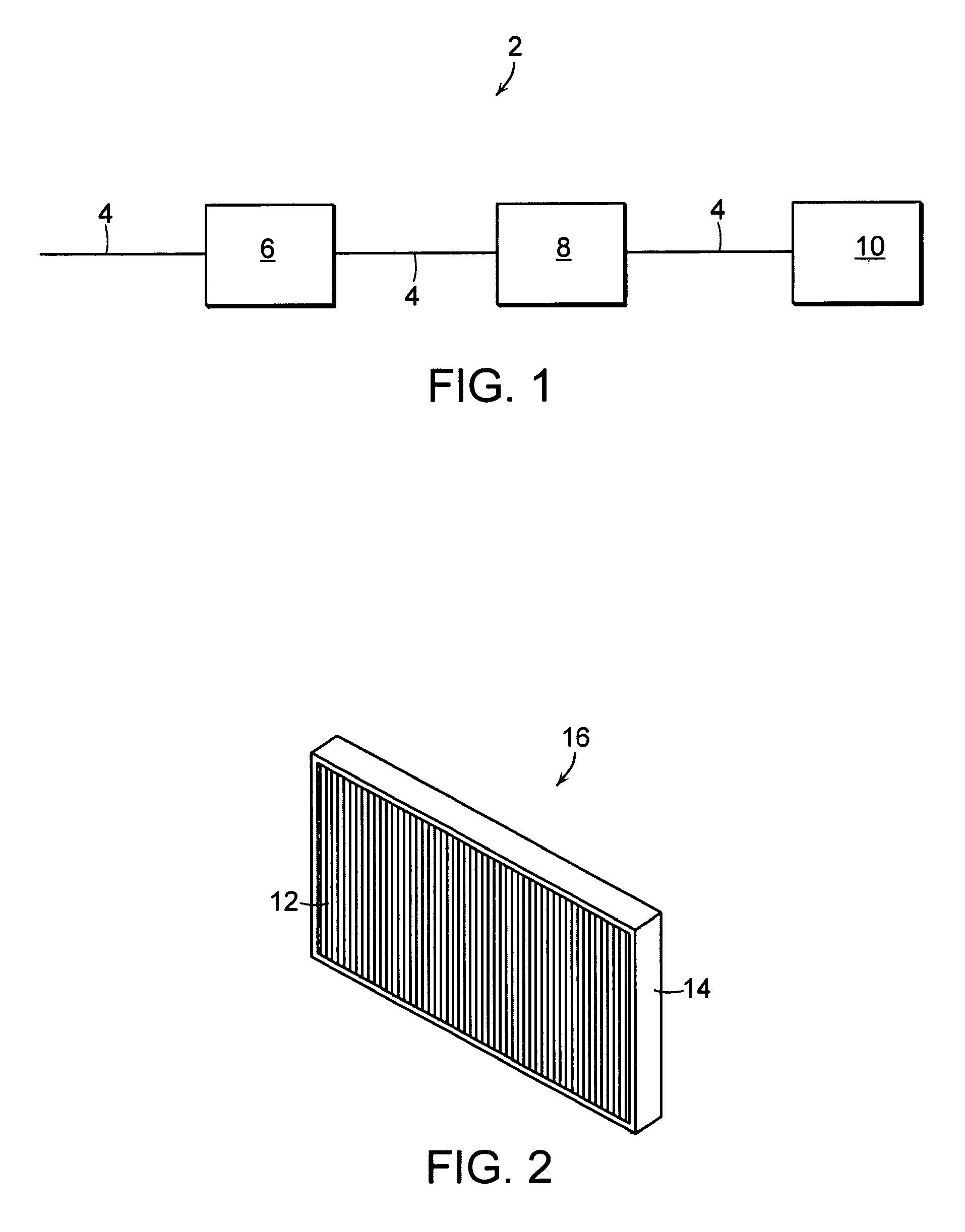
[0026]The invention provides a filtering system for a semiconductor processing tool. In a preferred embodiment, the filtering system is associated with the semiconductor processing tool. For example, the filtering system can be arranged to be mounted or coupled to the semiconductor processing tool. A system of the invention comprises a first and second filter layer in fluid communication with a gas flow path. The gas flow path passes through the first and second filter layer to fluidly communicate with the semiconductor processing tool. The first filter layer is upstream along the gas flow path from the second filter layer.

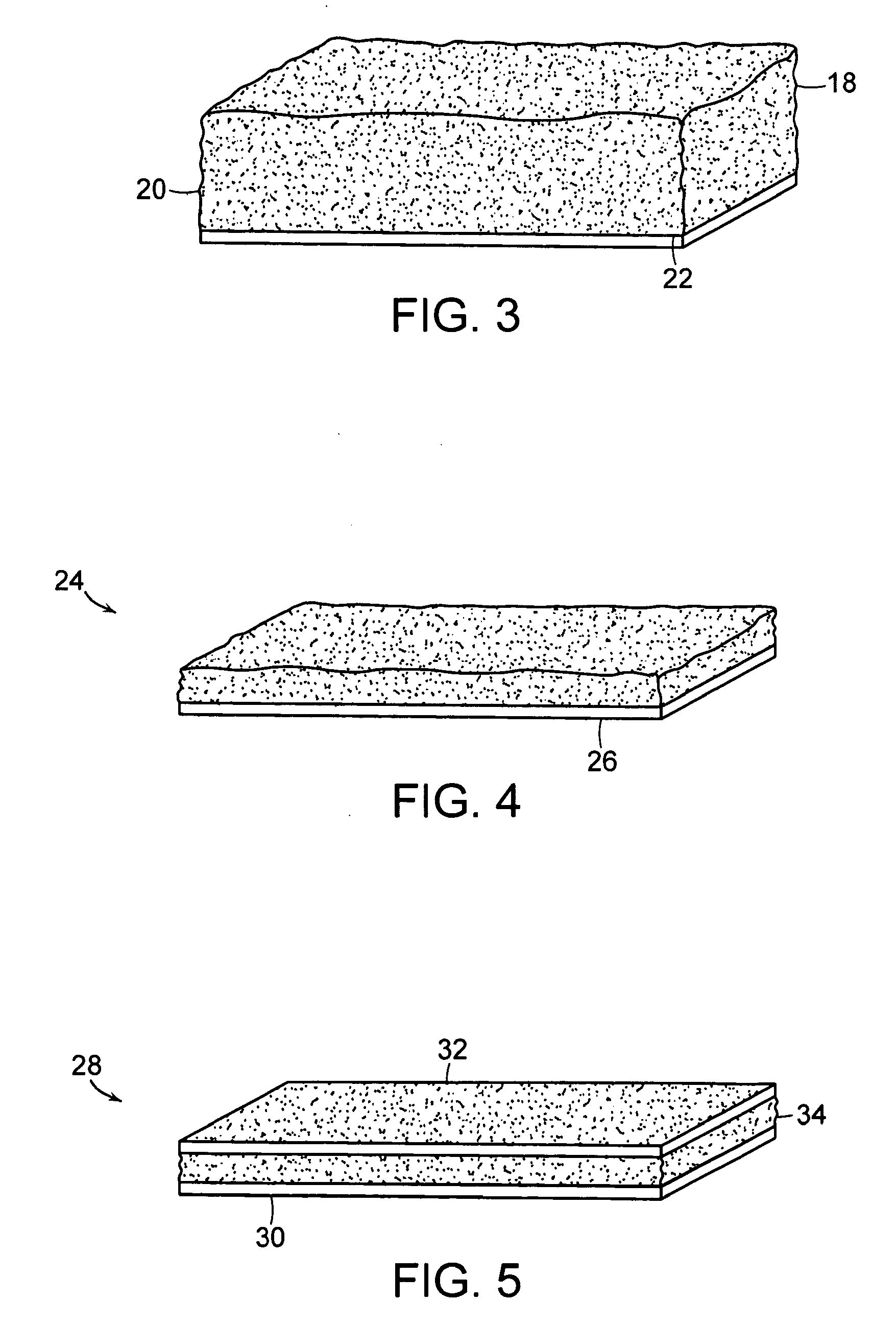
[0027]The medias of a first and second filter layer for a system of the invention are selected and arranged given particular contaminant concentrations. Preferably, with higher contaminant concentrations of hexamethyldisiloxane as compared to other volatile silica containing compounds, the first and second filter layers comprise physisorptive and chemisorptive med...


PUM

PropertyMeasurementUnit
Flow rateaaaaaaaaaa
Concentrationaaaaaaaaaa
Acidityaaaaaaaaaa

Abstract

The present invention provides a filtering system for a semiconductor processing tool. In one embodiment, the filtering system is associated with the semiconductor processing tool. A system of the invention comprises a first and second filter layer in fluid communication with a gas flow path. The flow path is a gas stream comprising volatile silica containing compounds such as hexamethyldisiloxane and trimethylsilanol. The gas flow path passes through the first and second filter layer to fluidly communicate with the semiconductor processing tool. Preferably, the first filter layer of the filtering system is upstream along the gas flow path from the second filter layer. The medias of the first and second filter layers are selected and arranged based on given contaminant concentrations. The invention also provides a method for filtering gas containing hexamethyldisiloxane and trimethylsilanol in communication with a semiconductor processing tool, which employs a system comprising a first and second filter layer.

Description

CROSS REFERENCE TO RELATED APPLICATIONS[0001]The present application claims priority to U.S. application No. 60 / 830,737, filed Jul. 13, 2006, the entire contents of which is incorporated herein by reference.BACKGROUND OF THE INVENTION[0002]The overall quality of gases is of growing concern within semiconductor manufacturing facilities. In general, tremendous efforts are made to eliminate yield reducing contaminants from air used for semiconductor processing tools. For example, contaminants are viewed as molecular compounds present in a gas that can inhibit semiconductor processing tool performance through deposit formations. With lithography tools, gases are employed to purge and actuate tool components. Contaminants such as volatile silica containing compounds in these gases are usually present at levels capable of damaging lithography tool optics.[0003]Typically, volatile silica containing compounds such as hexamethyldisiloxane and trimethylsilanol adhere to lithography tool optic...

Claims


Application Information

Patent Timeline
IPC IPC(8): B01D53/04B01D46/00B23P11/00
CPCB01D46/0023Y10T29/49826B01D53/0407B01D2253/102B01D2253/206B01D2257/553B01D2257/556B01D2257/708B01D2259/402B01D2259/414B01D2259/4148B01J20/20B01J20/28035B01J39/043B01D46/0036B01J39/05B01D46/62B01D53/04B01D46/00
Inventor GRAYFER, ANATOLYKISHKOVICH, OLEG P.
Owner ENTEGRIS INC
Why Eureka
Try Eureka