Coreless substrate package with symmetric external dielectric layers

a dielectric layer and coreless technology, applied in the field of substrates, can solve the problems of forming the layers on the core, unable to provide sufficient structural rigidity and appropriate thermal properties, and unable to create a coreless substra

Inactive Publication Date: 2009-12-31
INTEL CORP
View PDF6 Cites 30 Cited by
  • Summary
  • Abstract
  • Description
  • Claims
  • Application Information

AI Technical Summary

Problems solved by technology

Creating a coreless substrate, however, presents challenges in providing sufficient structural rigidity and appropriate thermal propert

Method used


Image

  • Coreless substrate package with symmetric external dielectric layers
  • Coreless substrate package with symmetric external dielectric layers
  • Coreless substrate package with symmetric external dielectric layers

Examples


Embodiment Construction

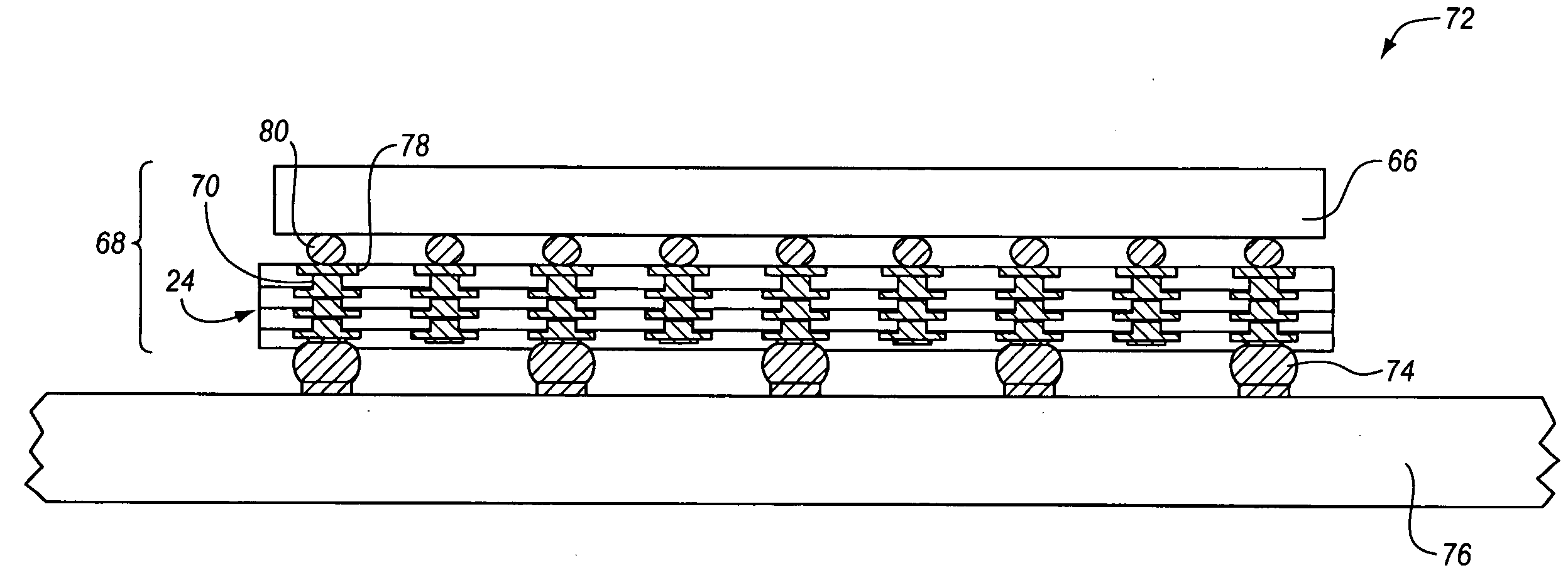
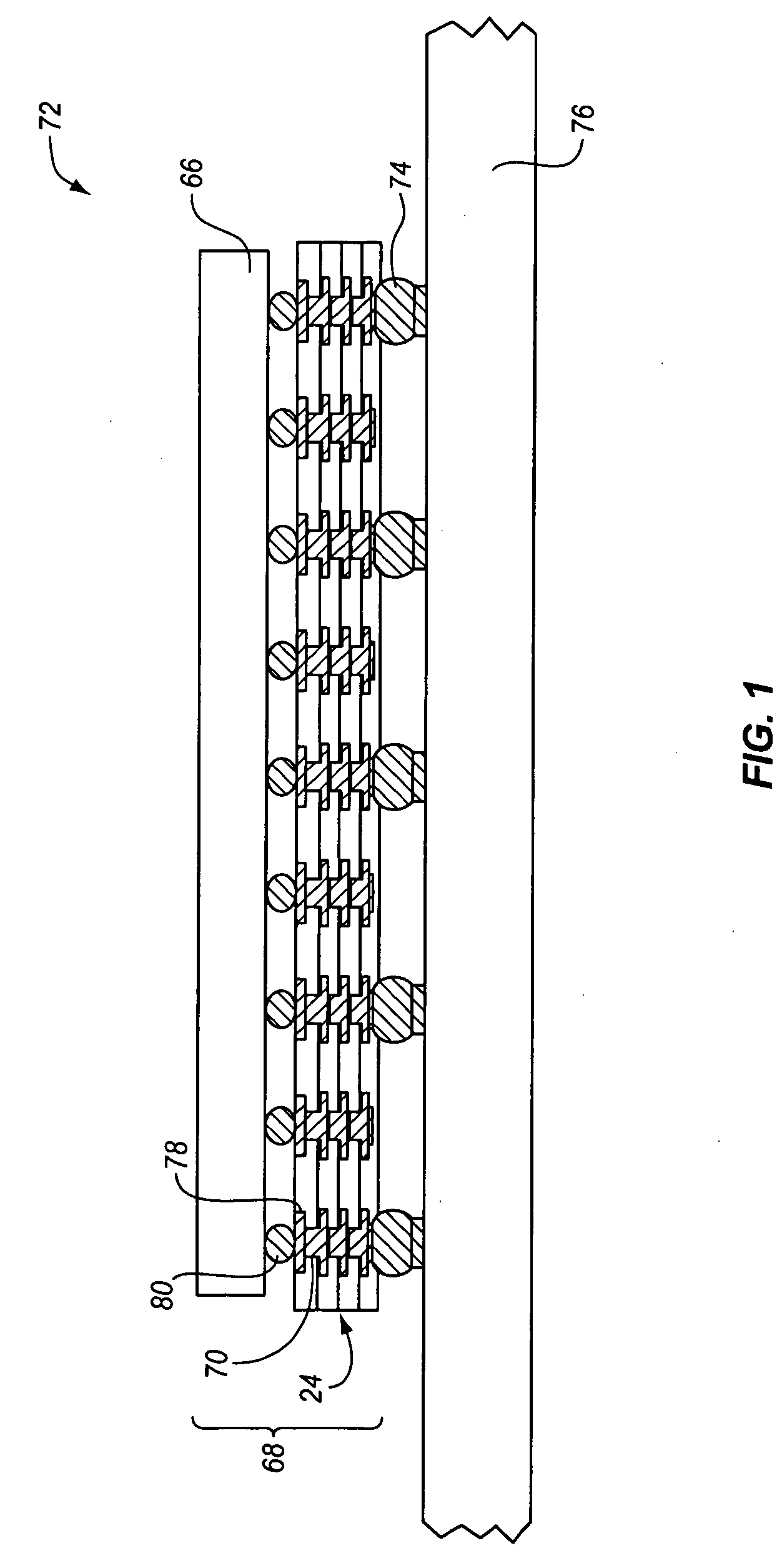
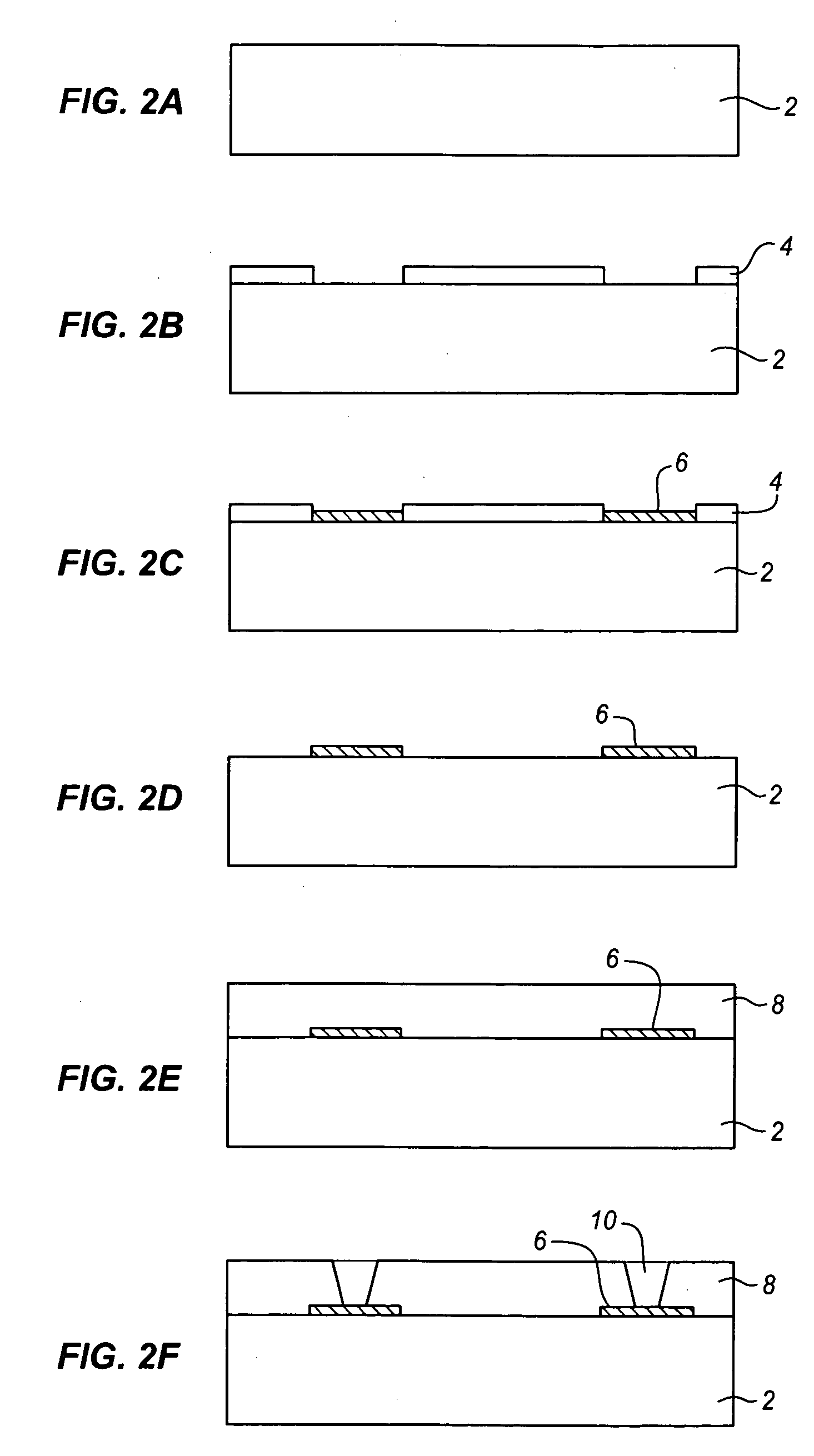
[0031]According to an embodiment of the invention, a protective step is used to separate a coreless substrate from the temporary core before the substrate is submitted to a SR (Solder Resist) process. Once separated, thin package SR may be used to transform the BE (Back End) of a coreless substrate to a standard building FCBGA (Flip Chip Ball Grid Array) process. This allows many conventional chemistry and processing steps to be used. It also allows coreless substrates routing to be formed on both sides of the substrate.

[0032]It may be difficult to produce coreless packages using existing materials. Some processes have been proposed which require new surface chemistry. A new surface chemistry imposes new capital investments for substrate suppliers, for developing experience and consistency, and for creating the surface finishes between top and bottom layers.

[0033]According to an embodiment of the invention, the assembly process may use a very similar external SR layer to substrates ...


PUM


Abstract

A thin die Package Substrate is described that may be produced using existing chemistry. In one example, a package substrate is built over a support material. A dry film photoresist layer is formed over the package substrate. The support material is removed from the package substrate. The dry film photoresist layer is removed from the substrate and the substrate is finished for use with a package.

Description

BACKGROUND[0001]1. Field[0002]The present description relates to the field of substrates for use in packaging and mounting semiconductor and micromechanical dies, and in particular to building coreless substrates over a temporary core and then removing the core prior to finishing the substrate.[0003]2. Related Art[0004]Integrated circuits and micromechanical structures are typically formed in groups on a wafer. The wafer is a substrate, typically of silicon or the like and then is cut up into dies, so that each die contains one integrated circuit or micromechanical structure. Each die is then mounted to a substrate and is then typically packaged. The substrate connects the die to a printed circuit board, socket or other connection. The package supports or protect the die and may also provide other functions such as isolation, insulation, thermal control and more.[0005]Substrates for this purpose are typically made of woven glass layers pre-impregnated with an epoxy resin material, s...

Claims


Application Information

Patent Timeline
IPC IPC(8): H01L23/48H01L21/4763H01L23/52H01L21/441H01L23/485H01L21/44
CPCH01L2221/68345H01L2224/16235H01L2924/01004H01L2924/01046H01L2924/01078H01L2924/01079H01L2924/14H01L2924/15311H05K3/205H05K3/243H05K3/4682H05K2203/0376H01L21/4857H01L21/6835H01L23/49822H01L24/16H01L2924/01087H01L2224/16H01L23/053
Inventor GONZALEZ, JAVIER SOTOWU, TAOALUR, PALLAVIROY, MIHIRLI, SHENGOLMEDO, REYNALDO
Owner INTEL CORP
Why Eureka
Try Eureka