Magnetic sensor

Inactive Publication Date: 2009-12-31
TDK CORPARATION
View PDF18 Cites 2 Cited by
  • Summary
  • Abstract
  • Description
  • Claims
  • Application Information

AI Technical Summary

Benefits of technology

[0028]These materials have a low electrical resistance and thus can favorably actualize the nonmagnetic low resistance layer in the magnetic sensor.
[0029

Problems solved by technology

Also, the resistance of the free magnetization layer per se may make it difficult to detect a voltage occurring in the part of the free magnetization layer overlapping the nonmagnetic conductive layer at a location remote from the end part not overlapping the nonmagnetic conductive l

Method used


Image

  • Magnetic sensor
  • Magnetic sensor
  • Magnetic sensor

Examples


first embodiment

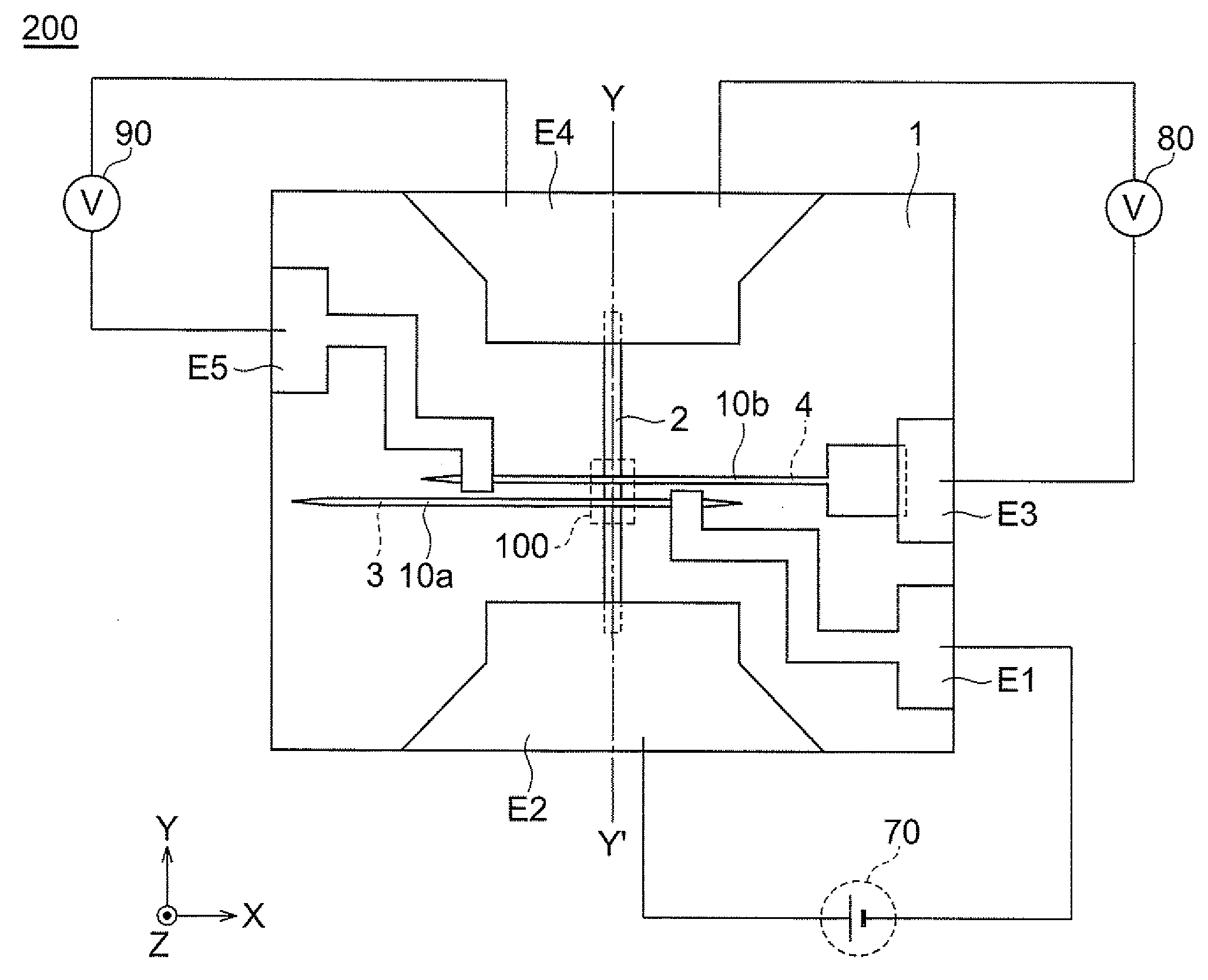
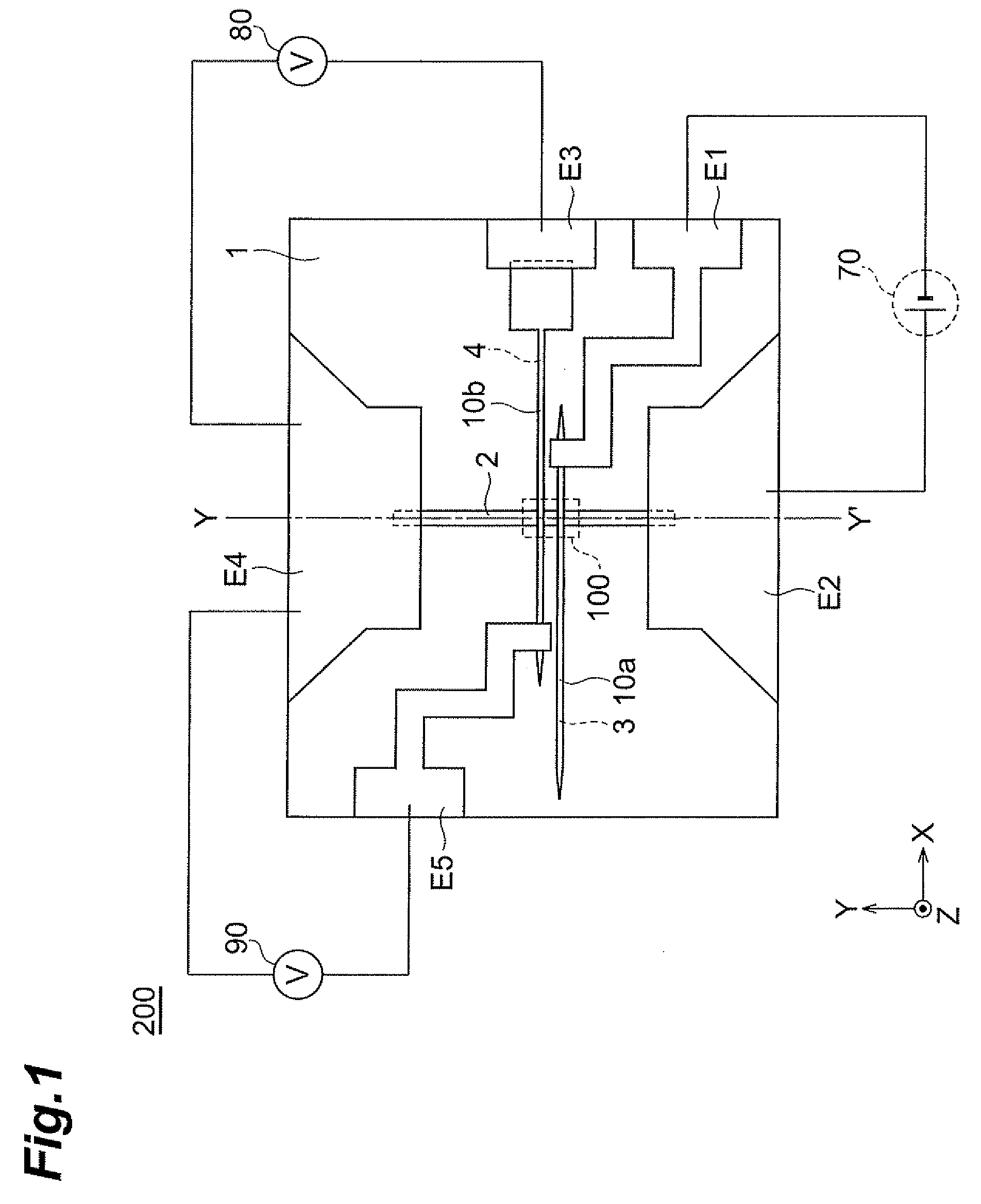
[0037]An example of the spin accumulation magnetic sensor in accordance with the first embodiment will now be explained.

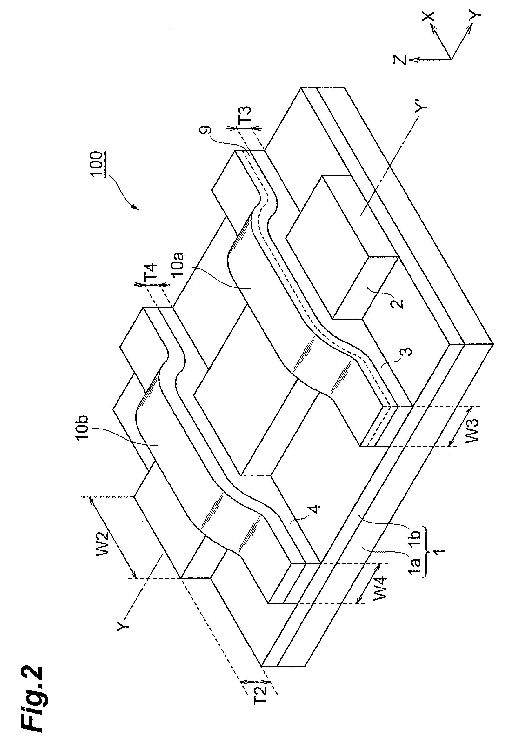
[0038]FIG. 1 is a schematic top plan view illustrating a magnetic sensor 200. FIG. 2 is a perspective view corresponding to a dashed box 100 in FIG. 1. The line Y-Y′ illustrated in FIG. 1 corresponds to the line YY′ of FIG. 2.

[0039]As illustrated in FIGS. 1 and 2, the magnetic sensor 200 mainly comprises a support 1, a nonmagnetic conductive layer 2 disposed thereon for accumulating spins of electrons, a fixed magnetization layer 3 disposed on a first part of the nonmagnetic conductive layer 2 and on the support 1, a free magnetization layer 4 disposed on a second part of the nonmagnetic conductive layer 2 different from the first part and on the support 1, a nonmagnetic low resistance layer 10a disposed on the fixed magnetization layer 3, and a nonmagnetic low resistance layer 10b disposed on the free magnetization layer 4.

[0040]Support

[0041]As the support 1, a su...

example 1

[0079]Method of Making Magnetic Sensor

[0080]First, a Cu film was formed on a support constituted by a substrate and a foundation film. Thus formed film was subsequently patterned by photolithography, so as to form a nonmagnetic conductive layer 2 having a rectangular form as illustrated in FIG. 3. The nonmagnetic conductive layer 2 had a length L2 in the longer axis direction (Y direction) of 20 μm, a length W2 in the shorter axis direction (X direction) of 0.5 μm, and a thickness T2 of 0.1 μm.

[0081]Then, a film (having a thickness of 50 nm) made of an alloy containing Co and Fe and a Cu film (having a thickness of 100 nm) were continuously formed on the nonmagnetic conductive layer 2 and patterned by photolithography, so as to form a fixed magnetic gap layer 3 and a nonmagnetic low resistance layer 10a each of which was shaped like a spear whose both end parts were pointed as illustrated in FIG. 4A, and a free magnetization layer 4 and a nonmagnetic low resistance layer 10b each of...


PUM


Abstract

A magnetic sensor comprises a support; a nonmagnetic conductive layer disposed on the support; a fixed magnetization layer disposed on a first part of the nonmagnetic conductive layer and on the support; a free magnetization layer disposed on a second part of the nonmagnetic conductive layer different from the first part and on the support; and a nonmagnetic low resistance layer, disposed on a part overlapping the nonmagnetic conductive layer in at least one of the fixed magnetization layer and free magnetization layer, having an electrical resistivity lower than that of the one layer.

Description

BACKGROUND OF THE INVENTION[0001]1. Field of the Invention[0002]The present invention relates to a magnetic sensor.[0003]2. Related Background Art[0004]As magnetic sensors used in thin-film magnetic recording and reproducing heads and the like, magnetoresistive (MR) devices have conventionally been known. In general, the MR devices cause a current to flow between a fixed magnetization layer and a free magnetization layer and thus attain high outputs. In the MR devices, however, domain wall movements due to spin torques given by the current and the like yield signals unnecessary for the magnetic sensors.[0005]On the other hand, a spin accumulation (SA) magnetic sensor in which a free magnetization layer and a fixed magnetization layer are formed on the same horizontal surface (nonmagnetic conductive layer for accumulating spins) has been known (see, for example, Japanese Patent Application Laid-Open No. 2007-299467 and Japanese Patent Publication No. 4029772). When a spin accumulatio...

Claims


Application Information

Patent Timeline
IPC IPC(8): G11B5/127
CPCY10T428/1121G01R33/1284G11B5/398B82Y25/00G01R33/093Y10T428/1143Y10T428/1107
Inventor SASAKI, TOMOYUKI
Owner TDK CORPARATION
Why Eureka
Try Eureka