

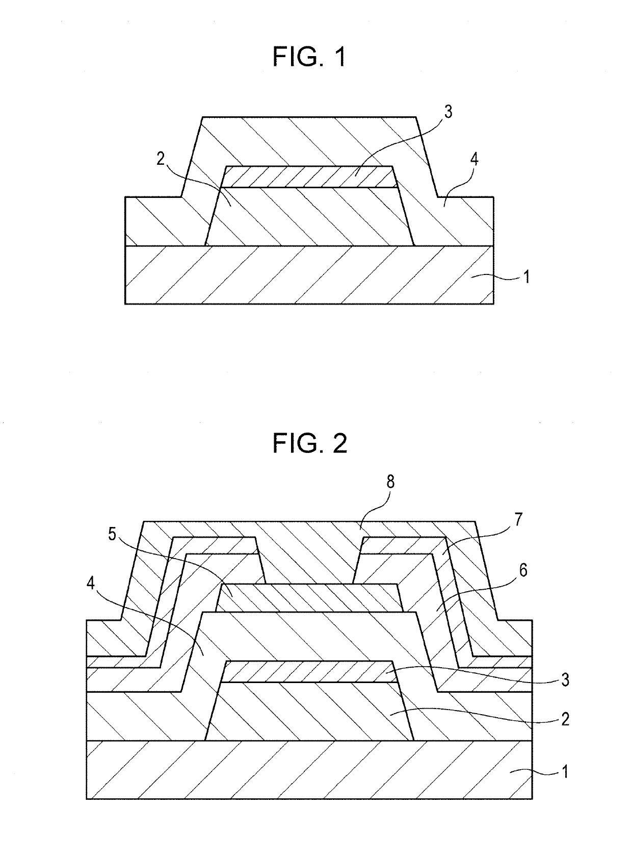
Multilayer wiring film and thin film transistor element
- Summary
- Abstract
- Description
- Claims
- Application Information
AI Technical Summary
Benefits of technology
Problems solved by technology
Method used
Image

Examples
example 1
(1) Production of Multilayer Wiring Film
[0079]An alkali-free glass plate having a diameter of 4 inches and a thickness of 0.7 mm was provided as a transparent substrate. The alkali-free glass plate was washed with a neutral detergent and then subjected to irradiation with an excimer UV lamp for 30 minutes to remove contamination on the surface. A multilayer wiring film including a wiring layer and a cap layer serving as a Cu—X alloy layer in Table 1 was formed on the surface-treated alkali-free glass plate by a DC magnetron sputtering method. The wiring film of the sample No. 1 was a single-layer film including only a wiring layer.
[0080]The atmosphere in a chamber was adjusted to 3×10⁻⁶ Torr once before film formation. Then, a wiring layer and a cap layer were formed on the substrate in this order by performing sputtering under the following sputtering conditions to form a multilayer wiring film. The sputtering target was a pure Cu sputtering target or a target having the same compo...
example 2
[0103]A multilayer wiring film using an adhesive layer containing Ti was produced through the following procedure. Specifically, as in Example 1, a multilayer wiring film including an adhesive layer, a wiring layer, and a cap layer serving as a Cu—X alloy layer in Table 2 was sequentially formed on the alkali-free glass plate serving as a transparent substrate by a DC magnetron sputtering method. The wiring film of the sample No. 40 is a multilayer film including only an adhesive layer and a wiring layer. The film formation conditions for the adhesive layer, the wiring layer, and the cap layer were the same as those in Example 1.
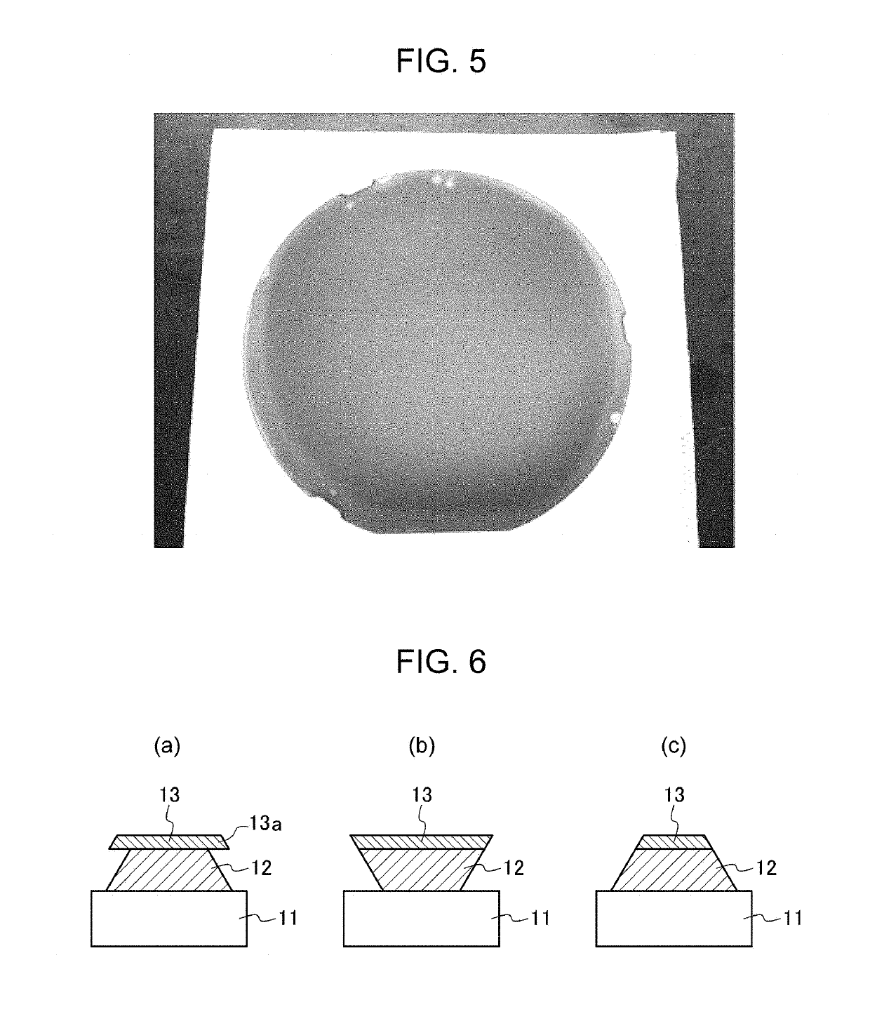
[0104]For the produced multilayer wiring films, the measurement of electrical resistivity and the evaluation of oxidation resistance were performed under the same conditions as those in Example 1. From the above results, samples in which the electrical resistivity after heat treatment at 400° C. is 3 μΩcm or less and film separation does not occur during for...
PUM
| Property | Measurement | Unit |
|---|---|---|
| Temperature | aaaaa | aaaaa |
| Length | aaaaa | aaaaa |
| Thickness | aaaaa | aaaaa |
Abstract
Description
Claims
Application Information