High-voltage metal-oxide-semiconductor transistor with shortened source and drain

a technology of metal-oxide-semiconductor transistors and source and drain, which is applied in the direction of code conversion, instruments, pulse techniques, etc., can solve the problems of disadvantageous increase in the layout area, and achieve the effect of reducing the layout area and shortening the source/drain region

Inactive Publication Date: 2010-01-14
HIMAX TECH LTD
View PDF6 Cites 0 Cited by
  • Summary
  • Abstract
  • Description
  • Claims
  • Application Information

AI Technical Summary

Benefits of technology

[0010]Accordingly, it is an object of the present invention to provide high-voltage metal-oxide-semiconductor transistors having shortened source / drain region, thereby substantially reducing the layout area.
[0011]It is another object of the present invention to provide decoders of the source driver of a liquid crystal display having reducing circuit layout area, while maintaining functionality and performance.

Problems solved by technology

Moreover, the occupying percentage of the layout area disadvantageously increases when the number of bits of the driver expands.

Method used


Image

  • High-voltage metal-oxide-semiconductor transistor with shortened source and drain
  • High-voltage metal-oxide-semiconductor transistor with shortened source and drain
  • High-voltage metal-oxide-semiconductor transistor with shortened source and drain

Examples


second embodiment

[0024]FIG. 6A shows a cross-section of a high-voltage N-type metal-oxide-semiconductor field-effect-transistor (HV NMOSFET or abbreviated as HV NMOS) 400 according to the present invention. Particularly, this HV MOSFET is used for, but not restricted to, implementing the decoders of the source drivers of the liquid crystal display. The HV MOS 400 includes a P-type semiconductor substrate 405, such as silicon substrate, on which gate oxide layers 402 are formed by a conventional process, such as oxidation. On the corresponding gate oxide layer 402 is a polysilicon (usually abbreviated as poly) layer 401, which is also formed by a conventional process, such as deposition. Consequently, a doped region 403 is formed in the substrate 405, and is disposed between the opposite edges of neighboring gate oxide layers 402. Specifically, in this embodiment, the doped region 403 acts as source / drain region, and is doped by N-type atoms having a doping concentration of about 1017 cm−3-1021 cm−3,...

third embodiment

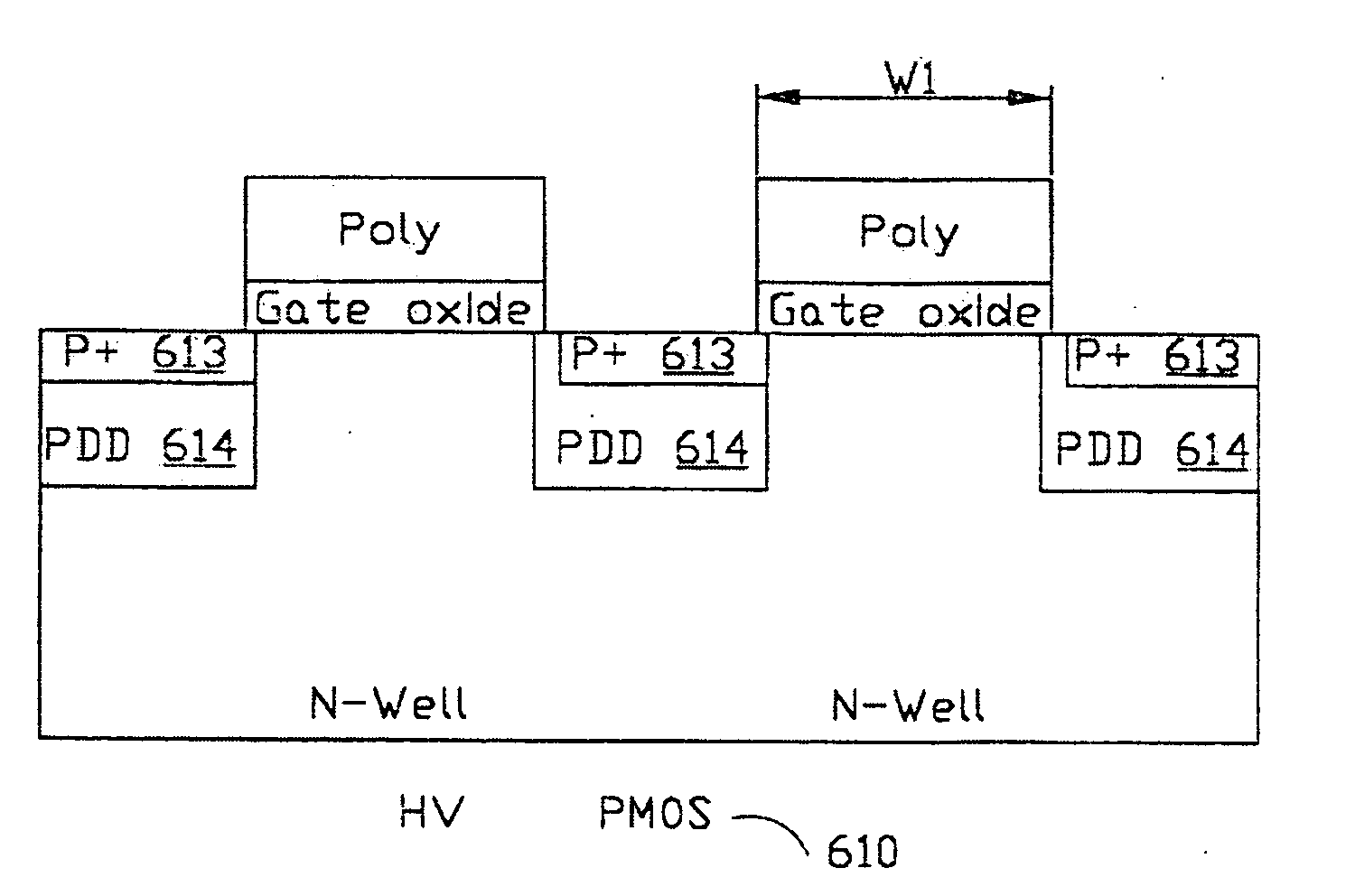
[0027]The present invention further discloses another embodiment as follows. FIG. 8A shows a cross-section of a high-voltage N-type metal-oxide-semiconductor field-effect-transistor (HV NMOSFET or abbreviated as HV NMOS) 600 according to the present invention. The structure of FIG. 8A is similar to that of FIG. 5A, except that an N+ region 603 is further formed within the NDD 604. In this embodiment, the N+ region 603 has a doping concentration of about 1017 cm−3-1021 cm−3, and the NDD 604 has a doping concentration of about 1014 cm−3-1020 cm−3. It is particularly noted that the overlapping percentage of the length of the N+ region 603 to the length of the NDD 604 could be 20% to 100%. More particularly, a portion of the N+ region 603 can be between the gate oxide and the NDD 604. Compared with standard process, the length of the NDD 604 is 1 to 5 times the length of the N+ region 603. According to the embodiment of the present invention, and comparing to that of FIG. 4A, the resist...


PUM


Abstract

A high-voltage metal-oxide-semiconductor (HV MOS) transistor is provided to form the decoder in a source driver of a display apparatus for substantially saving the layout area. The HV MOS transistor includes two doped regions with a first conductivity type disposed in a semiconductor substrate, and a gate region having a second conductivity type opposite to the first conductivity type on the semiconductor substrate and between the doped regions. Accordingly, the layout area could be substantially reduced.

Description

CROSS REFERENCE TO RELATED APPLICATIONS[0001]This application is a Continuation of co-pending application Ser. No. 12 / 203,044 filed Sep. 2, 2008, which is a Continuation of application Ser. No. 10 / 992,784 filed Nov. 22, 2004, now abandoned, the entire contents of all which are hereby incorporated by reference.BACKGROUND OF THE INVENTION[0002]1. Field of the Invention[0003]The invention relates to high-voltage metal-oxide-semiconductor transistors, and more particularly to high-voltage metal-oxide-semiconductor transistors utilized in a digital-to-analog circuit.[0004]2. Description of the Prior Art[0005]In a thin-film-transistor liquid crystal display (TFT LCD), the source driver receives digital image data 110 and transfers the digital image data 110 to analog image data 120, which are then outputted to the LCD panel, by the digital to analog converter (DAC) 130, as shown in FIG. 1. FIG. 2 illustrates the 3-bit N-type DAC, and the decoder 140 is included. A 3-bit P-type DAC looks s...

Claims


Application Information

Patent Timeline
Patent Type & Authority Applications(United States)
IPC IPC(8): H03M1/66H03K17/16
CPCH01L21/823425H01L29/7833H01L27/088
Inventor BU, LIN-KAICHEN, YING-LIEH
Owner HIMAX TECH LTD
Why Eureka
Try Eureka