Semiconductor temperature sensor

Inactive Publication Date: 2010-01-14
SEIKO INSTR INC
View PDF6 Cites 15 Cited by
  • Summary
  • Abstract
  • Description
  • Claims
  • Application Information

AI Technical Summary

Benefits of technology

[0010]According to the present invention, the leak current absorbing circuit absorbs the leak current included in the temperature detection current, and thus the leak current is less likely to flow th

Problems solved by technology

However, in the conventional semiconductor temperature sensors, not only the current according to the constant current of the constant current circuit but also a leak current of th

Method used


Image

  • Semiconductor temperature sensor
  • Semiconductor temperature sensor
  • Semiconductor temperature sensor

Examples


first embodiment

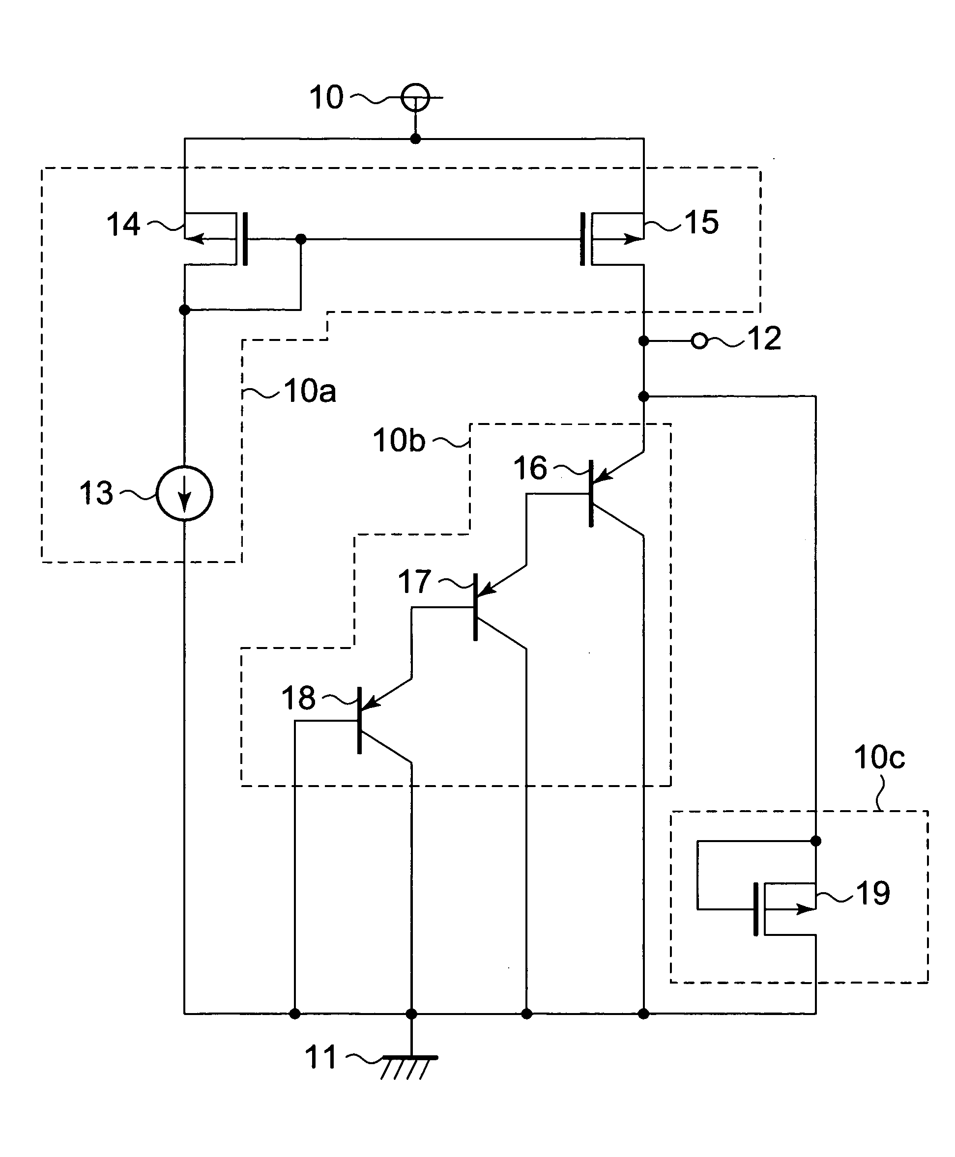
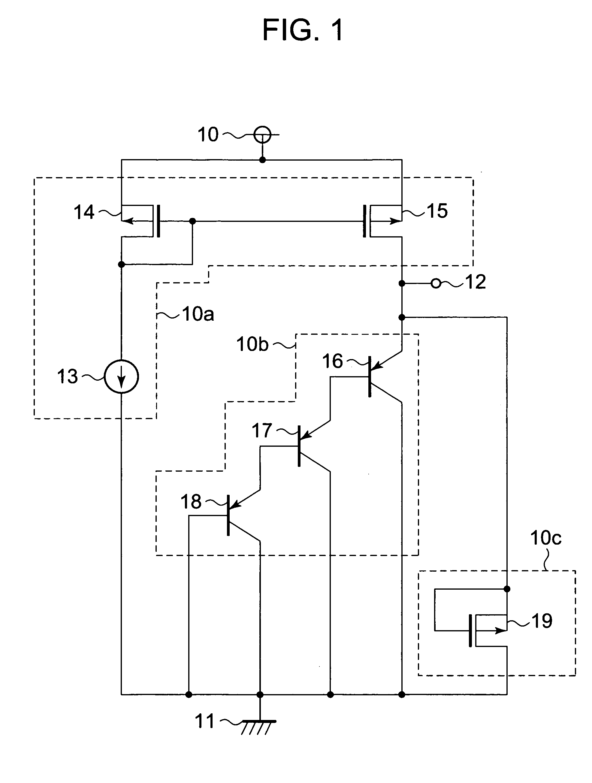
[0017]First, a configuration of a semiconductor temperature sensor is described. FIG. 1 is a circuit diagram illustrating a semiconductor temperature sensor according to a first embodiment of the present invention.

[0018]The semiconductor temperature sensor includes a constant current circuit 13, PMOS transistors 14 and 15, PNP bipolar transistors 16 to 18, and a PMOS transistor 19. The semiconductor temperature sensor further includes a power supply terminal 10, a ground terminal 11, and an output terminal 12.

[0019]The PMOS transistors 14 and 15 form a current mirror circuit. The constant current circuit 13 and the PMOS transistors 14 and 15 form a current supply circuit 10a. The PNP bipolar transistors 16 to 18 form a temperature detecting circuit 10b. The PMOS transistor 19 forms a leak current absorbing circuit 10c.

[0020]The PMOS transistor 14 has a gate and a drain connected to a gate of the PMOS transistor 15 and to an output terminal of the constant current circuit 13, and a ...

second embodiment

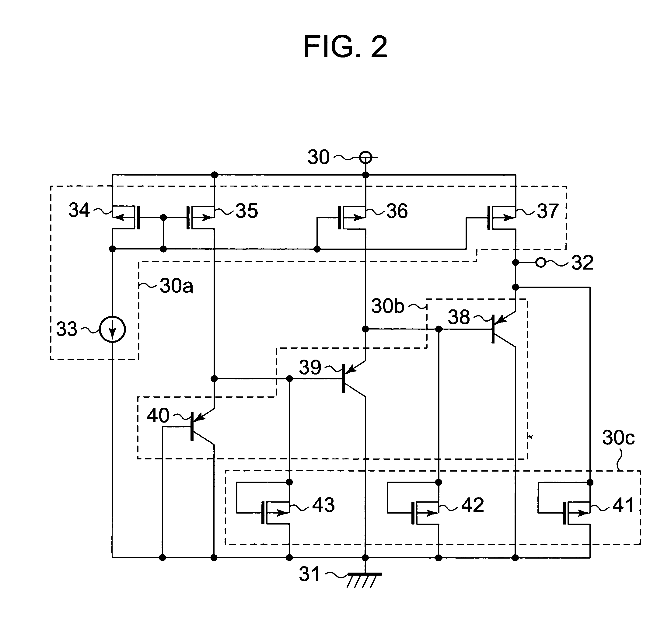
[0029]First, a configuration of the semiconductor temperature sensor is described. FIG. 2 is a circuit diagram illustrating a semiconductor temperature sensor according to a second embodiment of the present invention.

[0030]The semiconductor temperature sensor includes a constant current circuit 33, PMOS transistors 34 to 37, PNP bipolar transistors 38 to 40, and PMOS transistors 41 to 43. The semiconductor temperature sensor further includes a power supply terminal 30, a ground terminal 31, and an output terminal 32.

[0031]The PMOS transistors 34 to 37 form a current mirror circuit. The constant current circuit 33 and the PMOS transistors 34 to 37 form a current supply circuit 30a. The PNP bipolar transistors 38 to 40 form a temperature detecting circuit 30b. The PMOS transistors 41 to 43 form a leak current absorbing circuit 30c.

[0032]The PMOS transistor 34 has a gate and a drain connected to gates of the PMOS transistors 35 to 37 and to an output terminal of the constant current c...


PUM


Abstract

Provided is a semiconductor temperature sensor capable of enhancing accuracy of temperature detection. A constant current circuit (13) of a current supply circuit (10a) causes a constant current to flow. A current mirror circuit of the current supply circuit (10a) supplies a temperature detection current from an output terminal thereof according to the constant current of the constant current circuit (13). A temperature detecting circuit (10b) outputs an output voltage according to the temperature detection current and a temperature. A PMOS transistor (19) of a leak current absorbing circuit (10c) has the same size and conductivity type as those of a PMOS transistor (15), and absorbs a leak current included in the temperature detection current (drain current of the PMOS transistor (15)).

Description

BACKGROUND OF THE INVENTION[0001]1. Field of the Invention[0002]The present invention relates to a semiconductor temperature sensor.[0003]2. Description of the Related Art[0004]Description is made of conventional semiconductor temperature sensors are described. FIG. 3 is a circuit diagram illustrating a conventional semiconductor temperature sensor. FIG. 4 is a circuit diagram illustrating another conventional semiconductor temperature sensor.[0005]As illustrated in FIG. 3, a constant current circuit 53 causes a constant current to flow, and a current mirror circuit formed of PMOS transistors 54 and 55 causes a temperature detection current according to the constant current to flow through an emitter of a PNP bipolar transistor 56. A base current according to an emitter current of the PNP bipolar transistor 56 flows through an emitter of a PNP bipolar transistor 57, and a base current according to an emitter current of the PNP bipolar transistor 57 flows through an emitter of a PNP ...

Claims


Application Information

Patent Timeline
IPC IPC(8): G01K7/01
CPCG01K7/01
Inventor NOJIMA, KOJI
Owner SEIKO INSTR INC
Why Eureka
Try Eureka