Simulation buffer with voltage compensation mechanism

A voltage compensation and buffer technology, applied in instruments, regulating electrical variables, static indicators, etc., can solve problems such as complex control circuits, complex control signals, and the inability of analog buffers to meet requirements

Active Publication Date: 2008-09-17
AU OPTRONICS CORP
View PDF0 Cites 4 Cited by
  • Summary
  • Abstract
  • Description
  • Claims
  • Application Information

AI Technical Summary

Problems solved by technology

However, the above-mentioned traditional analog buffer requires quite a lot of control signals to control the on-off state of the switching element, and the current source also needs an additional current control signal, so the circuit operation of the traditional analog buffer essentially requires a complex control circuit to generate the complex control signals required
Therefore, for the design of thin and light liquid crystal display devices, the traditional analog buffer cannot meet the demand

Method used


Image

  • Simulation buffer with voltage compensation mechanism
  • Simulation buffer with voltage compensation mechanism
  • Simulation buffer with voltage compensation mechanism

Examples


Embodiment Construction

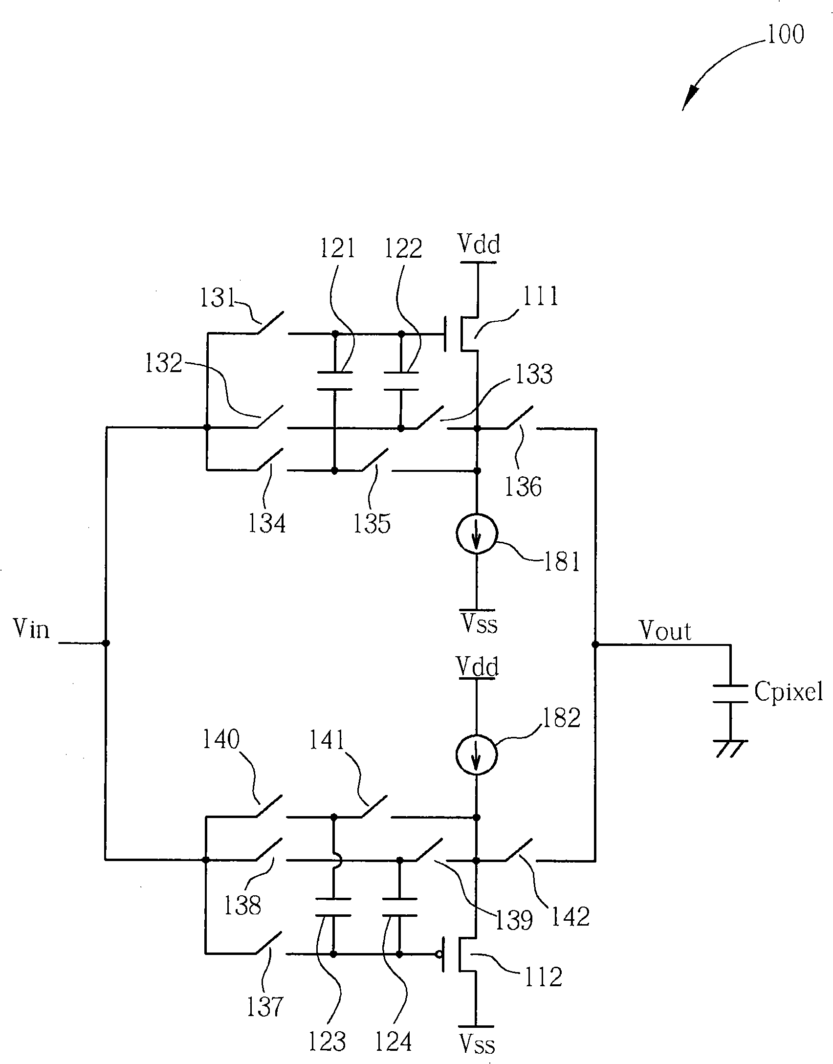
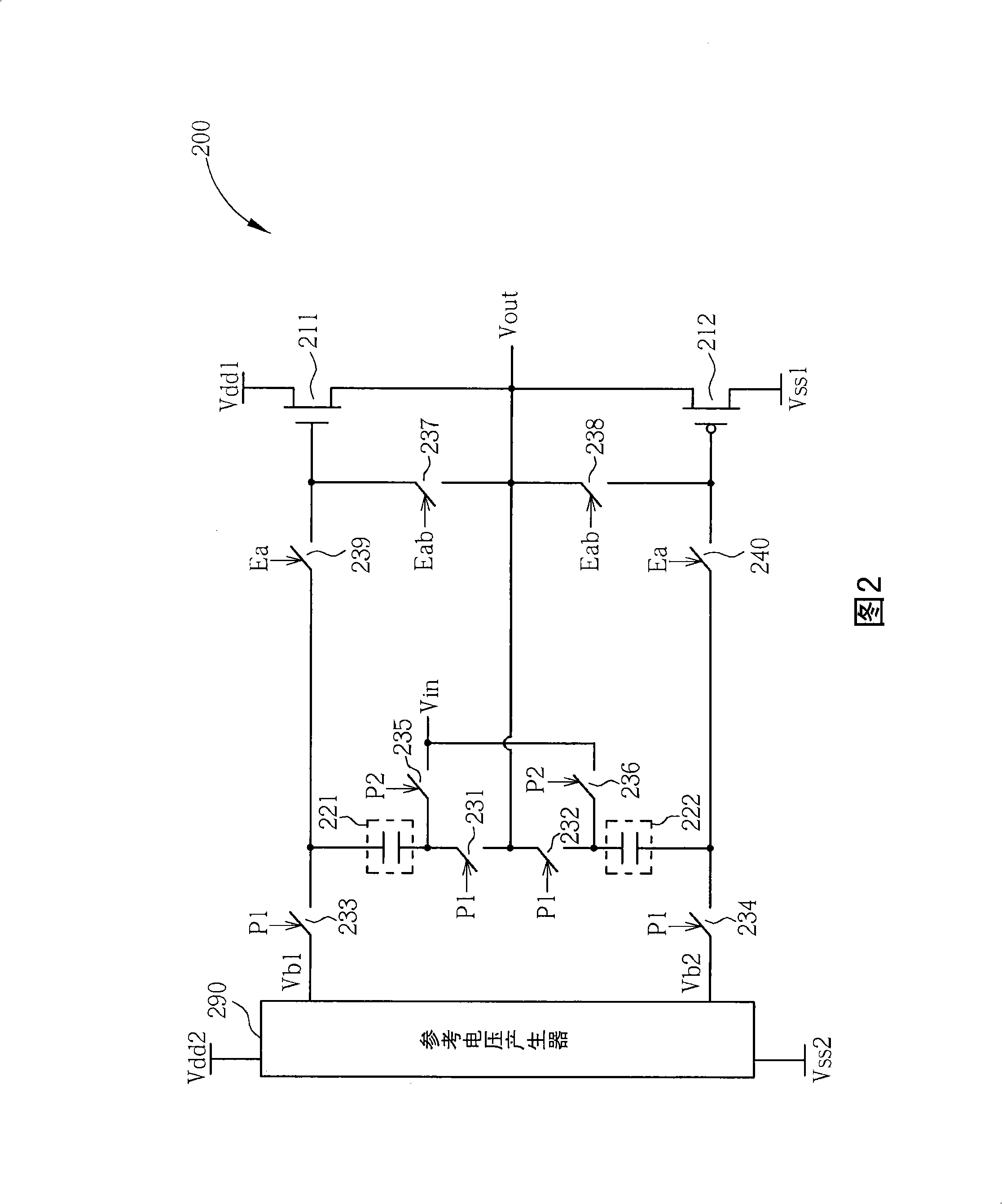
[0105] In order to make the present invention more comprehensible, the analog buffer with a voltage compensation mechanism according to the present invention will be described in detail below with reference to specific embodiments and accompanying drawings, but the provided embodiments are not intended to limit the scope of the present invention. scope.

[0106] FIG. 2 is a schematic diagram of an analog buffer circuit with a voltage compensation mechanism according to a first embodiment of the present invention. As shown in FIG. 2, the analog buffer 200 includes a first transistor 211, a second transistor 212, a first capacitor 221, a second capacitor 222, a first switch 231, a second switch 232, a third switch 233, a fourth switch 234, The fifth switch 235 , the sixth switch 236 , the seventh switch 237 , the eighth switch 238 , the ninth switch 239 , the tenth switch 240 , and the reference voltage generator 290 . The reference voltage generator 290 is powered by the third...


PUM


Abstract

An analog buffer which can be used for the source driving circuit of the liquid crystal display device and is provided with a voltage compensating mechanism comprises a reference voltage generator, a plurality of capacitances, a plurality of switches and a plurality of transistors. Through the reference voltage provided by the reference voltage generator, each capacitance can store the gate source pole voltage of the corresponding conducting transistor and is used for executing the gate source voltage compensating operation. Each switch controls the conducting cutoff state according to the corresponding control signal and further controls the compensation operation of the gate source voltage. Therefore the analog buffer of the invention has the function of compensating the gate source voltage of the conducting transistor and is used for reducing the error of the output voltage according to the input voltage to the allowable mini offset. Besides, the invention can reduce the power loss of the analog buffer and provides more accurate output voltage, and facilitates that the circuit of the analog buffer works in the signal voltage procession with a higher speed.

Description

technical field [0001] The invention relates to an analog buffer, in particular to an analog buffer with a voltage compensation mechanism. Background technique [0002] Liquid crystal display (Liquid Crystal Display; LCD) is a flat panel display widely used at present, which has the characteristics of light and thin appearance, power saving and no radiation. The working principle of the liquid crystal display device is to change the arrangement state of the liquid crystal molecules in the liquid crystal layer by changing the voltage difference between the two ends of the liquid crystal layer, so as to change the light transmittance of the liquid crystal layer, and then cooperate with the light source provided by the backlight module to display images. Generally speaking, a liquid crystal display device includes a plurality of pixel units, a plurality of data lines and a source driving device, and the source driving device includes a plurality of source driving circuits. Eac...

Claims


Application Information

Patent Timeline
Patent Type & Authority Applications(China)
IPC IPC(8): H03K19/0185G09G3/36G05F3/16
Inventor 陈忠君白承丘
Owner AU OPTRONICS CORP
Why Eureka
Try Eureka