
Image processing circuit and image display apparatus

Inactive Publication Date: 2010-02-04
SONY CORP
View PDF3 Cites 52 Cited by
  • Summary
  • Abstract
  • Description
  • Claims
  • Application Information

AI Technical Summary

Benefits of technology

[0009]It is desirable to provide an image processing circuit and an image display apparatus capable of improving contrast expression of a portion of an image that should be displayed particularly with high luminance level.
[0010]An image processing circuit according to an embodiment of the present invention includes: detecting means for detecting pixel regions where luminance levels of image signals exceed a given luminance threshold; and correcting means for applying basic gamma correction to image signals in regions other than the pixel regions detected, and applying luminance increasing gamma correction to image signals in the pixel regions detected, the luminance increasing gamma correction allowing the luminance levels to be increased.
[0011]An image processing circuit according to an embodiment of the present invention includes: a detecting unit detecting pixel regions where luminance levels of image signals exceed a given luminance threshold; and a correcting unit applying basic gamma correction to image signals in regions other than the pixel regions detected, and applying luminance increasing gamma correction to image signals in the pixel regions detected, the luminance increasing gamma correction allowing the luminance levels to be increased.
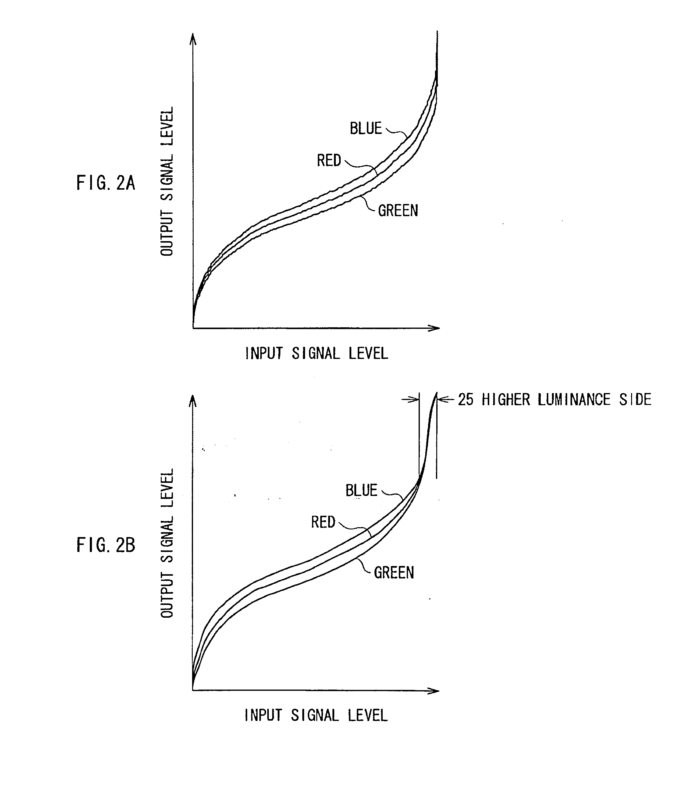
[0014]In the image processing circuit and the image display apparatus according to the embodiments of the present invention, the luminance increasing gamma correction (contrast enhancing process) is applied to the image signals in the pixel regions where the luminance levels of the image signals exceed the given luminance threshold (highlight portion), and the usual gamma correction is applied to the image signals in the regions other than the pixel regions detected. As a result, the highlight portion within an image is emphasized more and contrast expression improves.

Problems solved by technology

However, the above-mentioned white level expansion art does not always realize a satisfactory image quality of display.
For example, when an image includes a localized shiny object portion such as neon lights of night view, the moon of night sky or reflection of lighting that are shining brightly, it is difficult to fully express the brightness thereof, thus contrast expression falls short of reality.
Thus, even though red and green may be displayed with higher luminance, their luminance level is suppressed with a waste of surplus capability.
As a result, it is difficult to have a good contrast expression using the mixture of those three colors.
However, this technique merely applies the luminance correction independently to a predetermined portion of the display image to suppress the luminance irregularity, chromaticity unevenness, etc. within the display image, which are caused by the production tolerance of the display elements and the luminous energy distribution of back lights, etc., and the luminance correction is not performed dynamically in accordance with contents of the image.
Thus, when the image includes a localized shiny object portion that is shining brightly, it is also difficult to express the brightness thereof with reality.

Method used


Image

  • Image processing circuit and image display apparatus
  • Image processing circuit and image display apparatus
  • Image processing circuit and image display apparatus

Examples


first embodiment

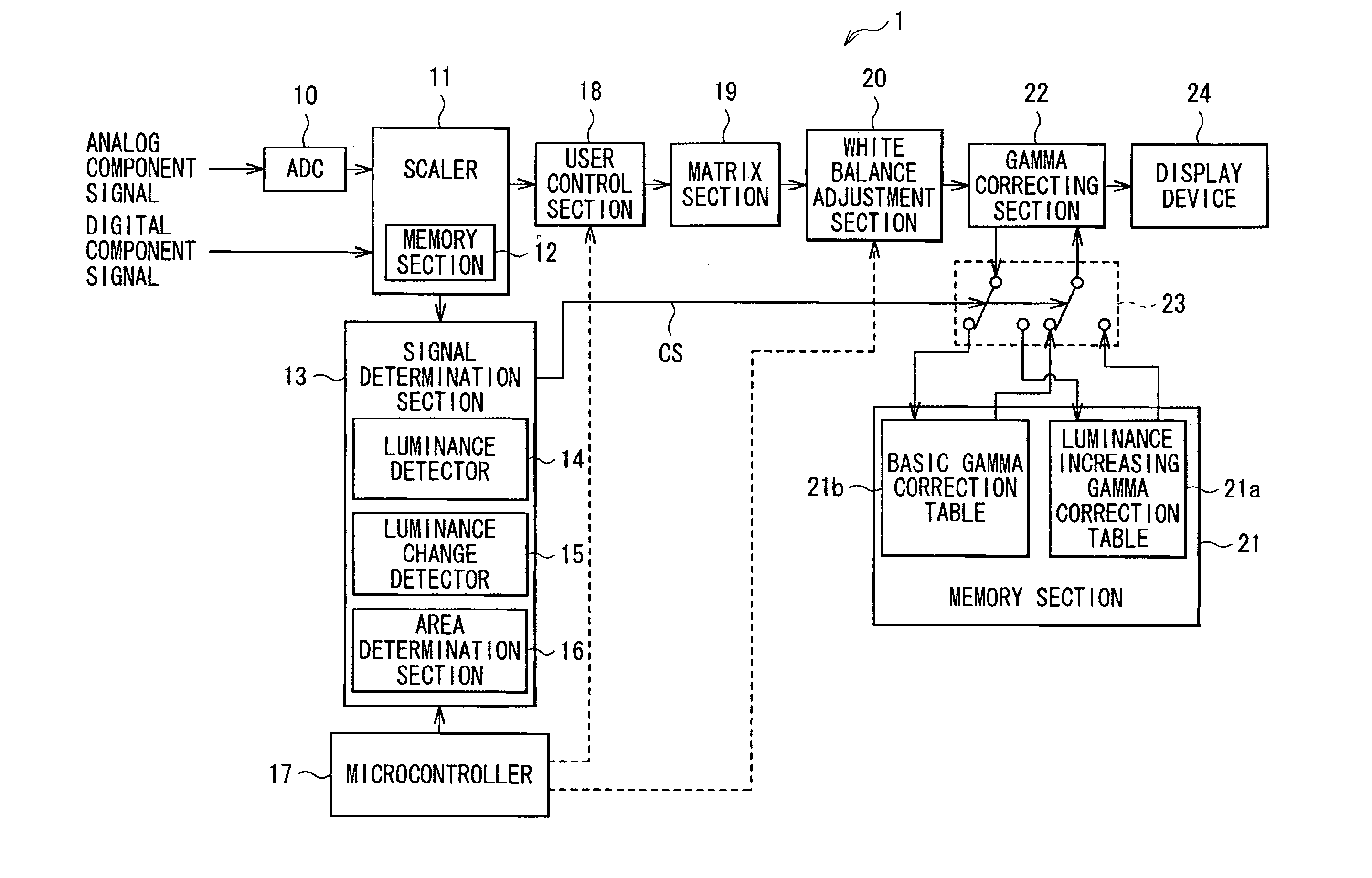
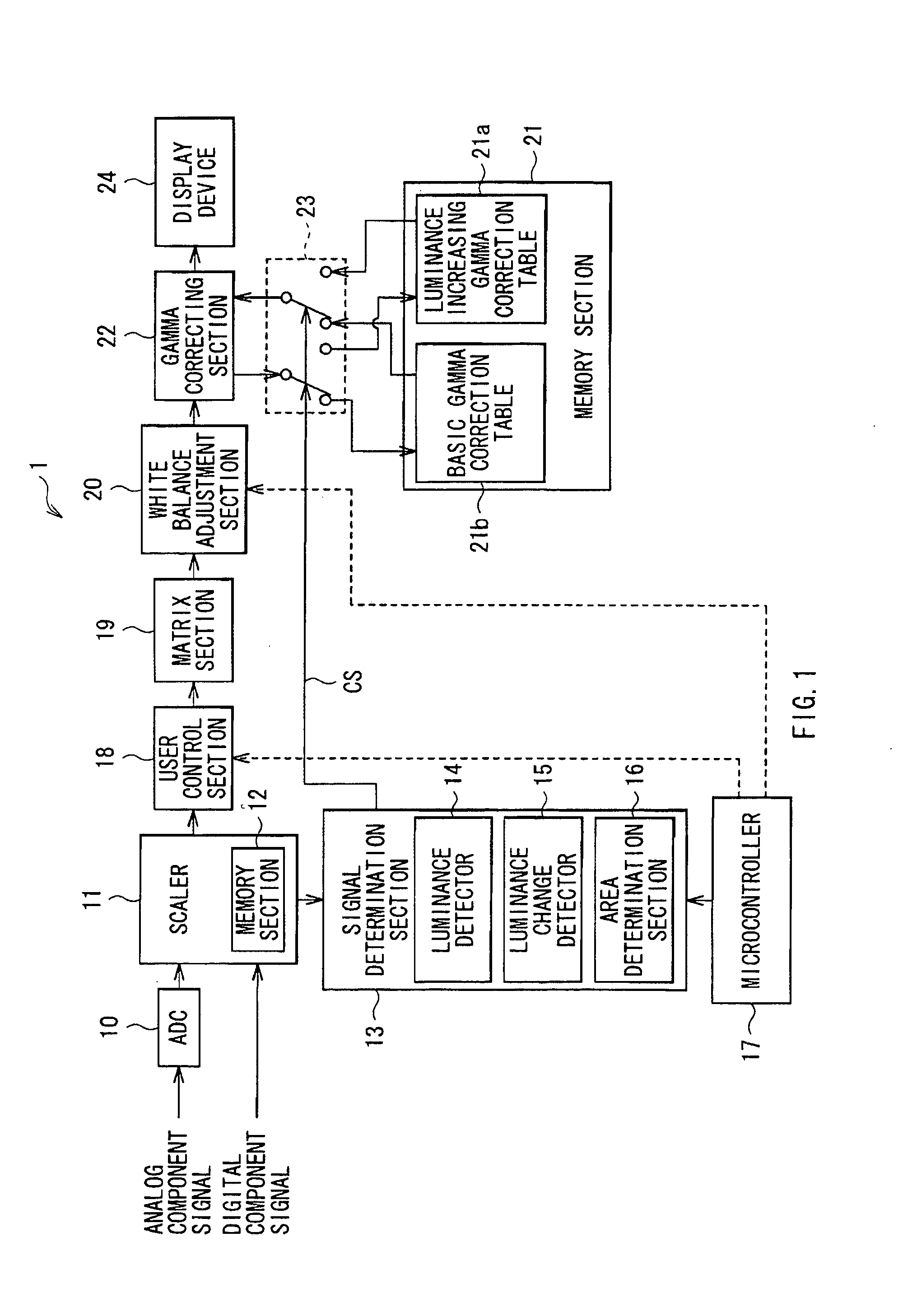
[0028]FIG. 1 is a configuration block of an image display apparatus including an image processing circuit according to the present invention. FIGS. 2A and 2B represent gamma correction tables to be hereinafter described.

[0029]The image display apparatus 1 includes an analog-to-digital converter (ADC) 10, a scaler 11, a signal determination section 13, a microcontroller 17, a user control section 18, a matrix section 19, a white balance adjustment section 20, a memory section 21, a gamma correcting section 22, and a display device 24. Here, the signal determination section 13 and the gamma correcting section 22 mainly corresponds to a specific example of the image processing circuit according to the embodiment of the invention.

[0030]ADC10 converts an analog component signal into a digital component signal. The scaler 11 selects either one of a component signal directly inputted from outside and a component signal outputted from the ADC10, and performs scaling of image size to be suit...

second embodiment

[0054]FIG. 4 illustrates a schematic configuration of an image display apparatus according to the present invention. FIGS. 5A and 5C illustrate gamma correction tables, and FIG. 5B illustrates a correction function.

[0055]The image display apparatus 2 according to the present embodiment is different from the image display apparatus 1 of the first embodiment in that the switch section 23 and the memory section 21 are replaced by an operation control section 31 and a memory section 30.

[0056]The memory section 30 stores therein only the basic gamma correction table 21b. The operation control section 31 creates the luminance increasing gamma correction table (FIG. 5C) by reading out the basic gamma correction table 21b from the memory section 30 and modulating its gamma characteristics with correction function. The correction function is stored in a correction function memory section 32 provided in the operation control section 31, and is read out therefrom at the time of operation.

[0057...


PUM


Abstract

An image processing circuit includes: a detecting unit detecting pixel regions where luminance levels of image signals exceed a given luminance threshold; and a correcting unit applying basic gamma correction to image signals in regions other than the pixel regions detected, and applying luminance increasing gamma correction to image signals in the pixel regions detected. The luminance increasing gamma correction allows the luminance levels to be increased.

Description

BACKGROUND OF THE INVENTION[0001]1. Field of the Invention[0002]The present invention relates to an image display apparatus which typically includes a liquid crystal display element, an organic electro luminescence element, etc., and to an image processing circuit applied to such image display apparatus. In particular, the invention relates to an image processing circuit and an image display apparatus to which an image quality improvement technology is applied.[0003]2. Description of the Related Art[0004]An image display apparatus such as a liquid crystal display element, an organic electro luminescence element, etc. adopts arts of whiteout prevention and white level expansion, etc. for improving image quality. Whiteout prevention is an art of preventing the detail of an image from being lost in highlight area, which is attained by detecting the maximum luminance of luminance signals and if the luminance level is saturated, reducing the luminance intensity with gamma correction. The...

Claims


Application Information

Patent Timeline
IPC IPC(8): G09G5/10
CPCG09G5/04H04N9/69G09G2320/0276G09G2320/0242
Inventor KONUMA, YASUSHI
Owner SONY CORP
Learn More