Display apparatus and driving device for displaying

Inactive Publication Date: 2006-02-28
PANASONIC LIQUID CRYSTAL DISPLAY CO LTD +1
View PDF7 Cites 6 Cited by
  • Summary
  • Abstract
  • Description
  • Claims
  • Application Information

AI Technical Summary

Benefits of technology

[0014]An object of the present invention is to provide a display

Problems solved by technology

In the case where the output of the gate driver is used for a panel configured of an additional capacitor Cadd, for example, the black display brightness of normally black liquid crystal increases, thereby sometimes making it impossible to obtain the proper contrast.
This abnormal increase in display brightness is attributable to the fact that the liquid panel is configure

Method used


Image

  • Display apparatus and driving device for displaying
  • Display apparatus and driving device for displaying
  • Display apparatus and driving device for displaying

Examples


first embodiment

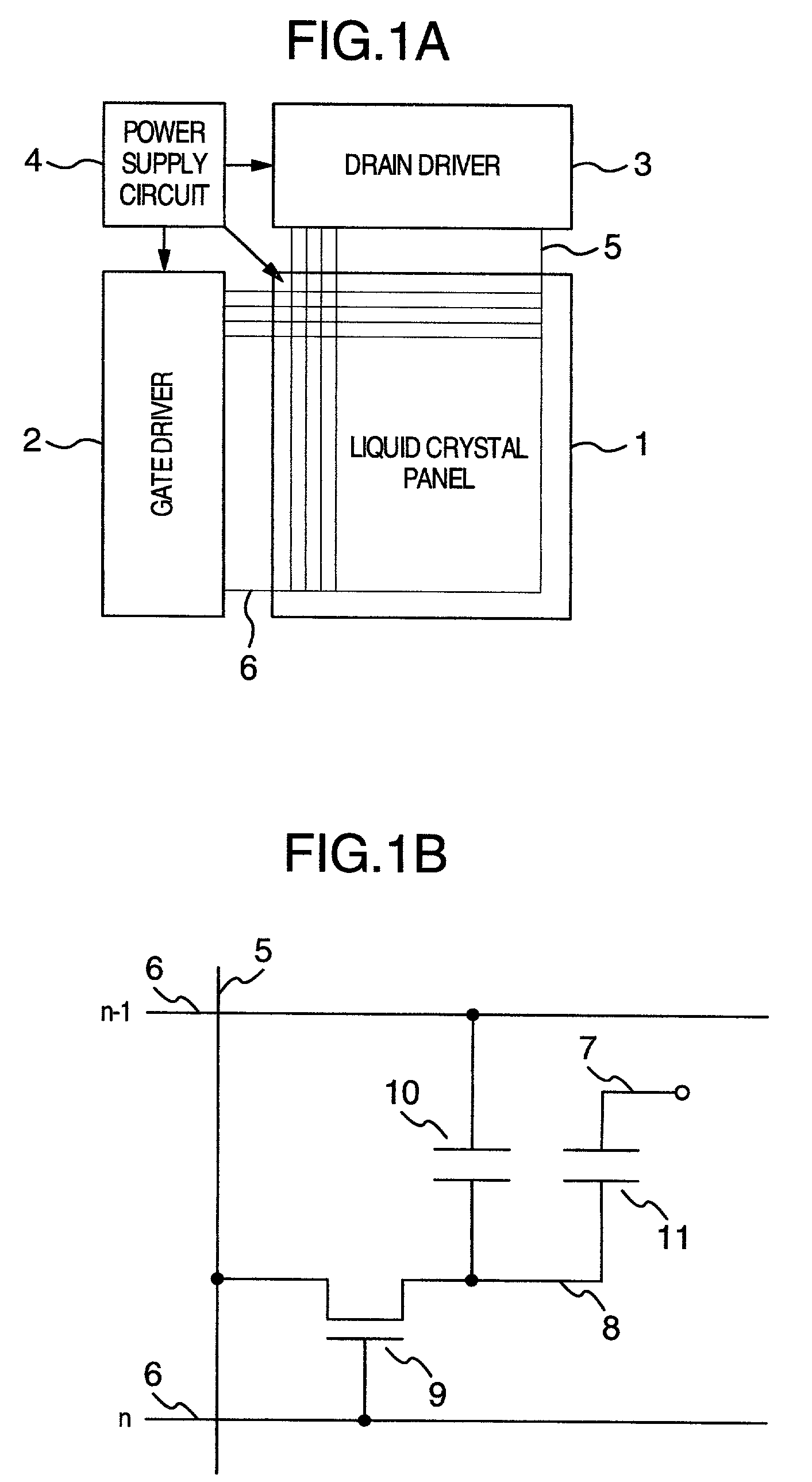
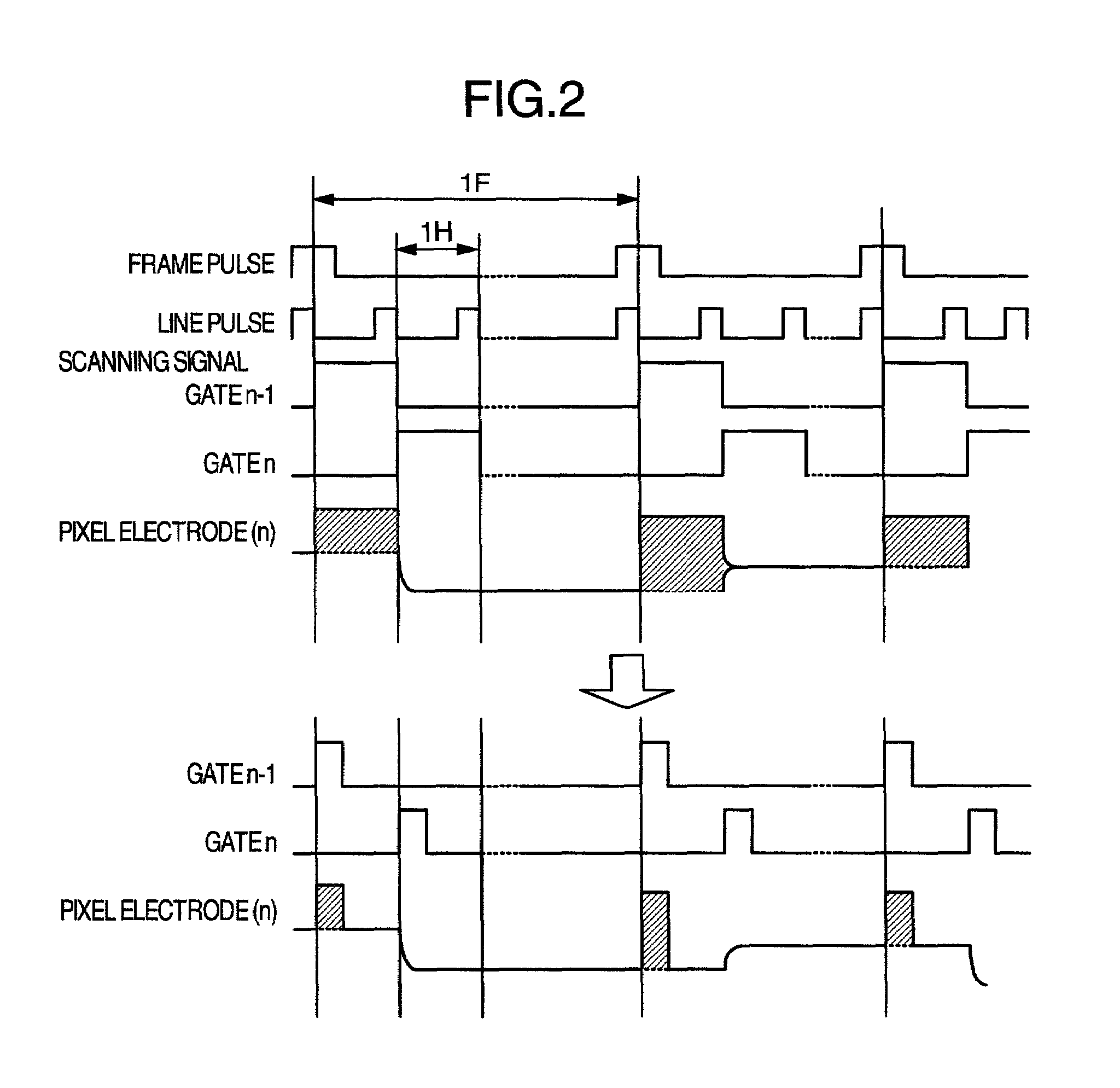
[0039]FIG. 4 is a block diagram showing a gate line drive circuit according to the invention. Reference numeral 801 designates a gate pulse signal, numeral 802 a scan data generating circuit for generating scan data, numeral 803 a level shifter, numeral 804 a gate line drive unit for outputting a gate pulse, numeral 805 a line pulse signal, numeral 806 a frame pulse signal and numeral 807 a pulse width signal. The gate driver 2 is supplied with the line pulse signal 805, the frame pulse signal 806 and the gate pulse width signal 807. The period of the pulse width signal 807 is equal to one horizontal period, and the high-level width (the time width during which the signal remains at high level) thereof is equal to the gate pulse width.

[0040]Based on the frame pulse signal 806 and the line pulse signal 805 input thereto, the scan data generating circuit 802 generates a timing of application of a gate line select voltage. In the case under consideration, the gate line select voltage i...

second embodiment

[0045]A gate line drive circuit according to the invention will be explained with reference to FIGS. 6 to 9.

[0046]FIG. 6 is a block diagram showing the gate line drive circuit according to the second embodiment of the invention. According to this invention, the gate pulse width is reduced by providing a non-overlap period (the period during which the select voltage is not input to any gate line). The gate pulse width can be varied by making the non-overlap period adjustable.

[0047]Numeral 808 designates a reference clock signal, numeral 809 information on a non-overlap period during which the select voltages for all the gate lines turn off, numeral 810 a non-overlap period generating unit for generating a non-overlap period waveform, and numeral 811 a register for storing the non-overlap period information 809. In place of the non-overlap period, the non-overlap timing (the timing of the gate pulse fall) may be set in a register. Also, in place of the non-overlap period, the time len...

third embodiment

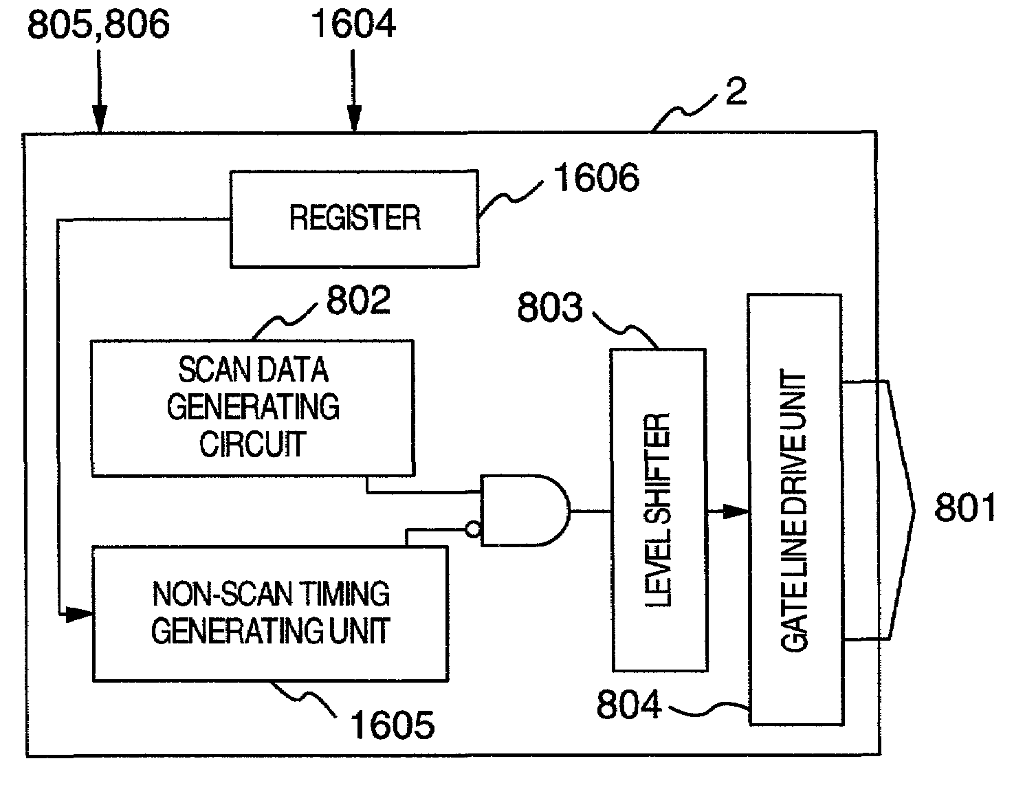
[0063]FIG. 12 is a block diagram showing the gate line drive circuit according to the invention.

[0064]Numeral 1604 designates a partial LCD drive function information for partial display, numeral 1605 a non-scan timing generating unit for generating a non-scan timing for partial display, and numeral 1606 a register for storing the partial LCD drive function information 1604.

[0065]The gate driver 2 is supplied with the frame pulse signal 806, the line pulse signal 805 and the partial LCD drive function information 1604. The partial LCD drive function information 1604 includes a start line SS and an end line SE of the display area, and a scanning rate SCN of the non-display area (n=SCN). In the description that follows, the scanning rate is assumed to be once for every n frames.

[0066]The partial LCD drive function information 1604 input from an external source is stored in the register 1606. The data on the start line SS and the end line SE of the display area and the scanning rate n ...


PUM


Abstract

A display apparatus and a display drive circuit are disclosed. The display drive circuit comprises a gate line drive circuit and a register. The gate line drive circuit outputs to the pixels a select voltage for selecting the pixels and a non-select voltage for prohibiting the selection of the pixels during one horizontal period. The register sets a non-overlap period for outputting a non-select voltage to at least two lines of pixels on the display panel during one horizontal period.

Description

BACKGROUND OF THE INVENTION[0001]The present invention relates to a display apparatus comprising a display panel with display pixels arranged in matrix, and a display drive circuit for selecting the display pixels to be impressed with a gray scale voltage, or in particular to a display apparatus employing liquid crystal, organic EL or plasma and a display drive circuit therefor.[0002]According to JP-A-6-161390 (laid open Jun. 7, 1994), a liquid crystal material is sealed between each of a plurality of pixel electrodes and a corresponding one of opposed electrodes, and the pixel electrodes are each connected with a switching transistor. A scanning signal for turning on / off the switching transistor is applied from a scanning signal supply circuit through a scanning signal line to the switching transistor. An image signal is supplied from an image signal supply circuit through an image signal line and the switching transistor to each pixel electrode. The scanning signal on an adjacent ...

Claims


Application Information

Patent Timeline
IPC IPC(8): G09G5/00G02F1/133G09G3/00G09G3/20G09G3/36
CPCG09G3/3659G09G2330/021G09G2310/065G09G3/3677
Inventor AKAI, AKIHITOKUDO, YASUYUKIOOKADO, KAZUOKUROKAWA, KAZUNARIHIGA, ATSUHIRO
Owner PANASONIC LIQUID CRYSTAL DISPLAY CO LTD
Why Eureka
Try Eureka