Method for Disposing Power/Ground Plane of PCB

Inactive Publication Date: 2010-02-04
KING YUAN ELECTRONICS
View PDF5 Cites 2 Cited by
  • Summary
  • Abstract
  • Description
  • Claims
  • Application Information

AI Technical Summary

Benefits of technology

[0009]In view of the prior art and some benefit-oriented demands of the industry, one objective of the present invention is to provide a method for determining whether via hole on

Problems solved by technology

Although it is easy to manufacture this kind of printed circuit board, yet the manufacturing process is too complex and the thickness and also production cost of multi-layer printed circuit board cannot be effectively reduced.
When the layout on the printed circui

Method used


Image

  • Method for Disposing Power/Ground Plane of PCB
  • Method for Disposing Power/Ground Plane of PCB
  • Method for Disposing Power/Ground Plane of PCB

Examples


Example

[0019]In order to disclose the skills applied in, the objectives of, and the effects achieved by the present invention in a more complete and clearer manner, preferred embodiments are herein described in detail below with related drawings disclosed for reference.

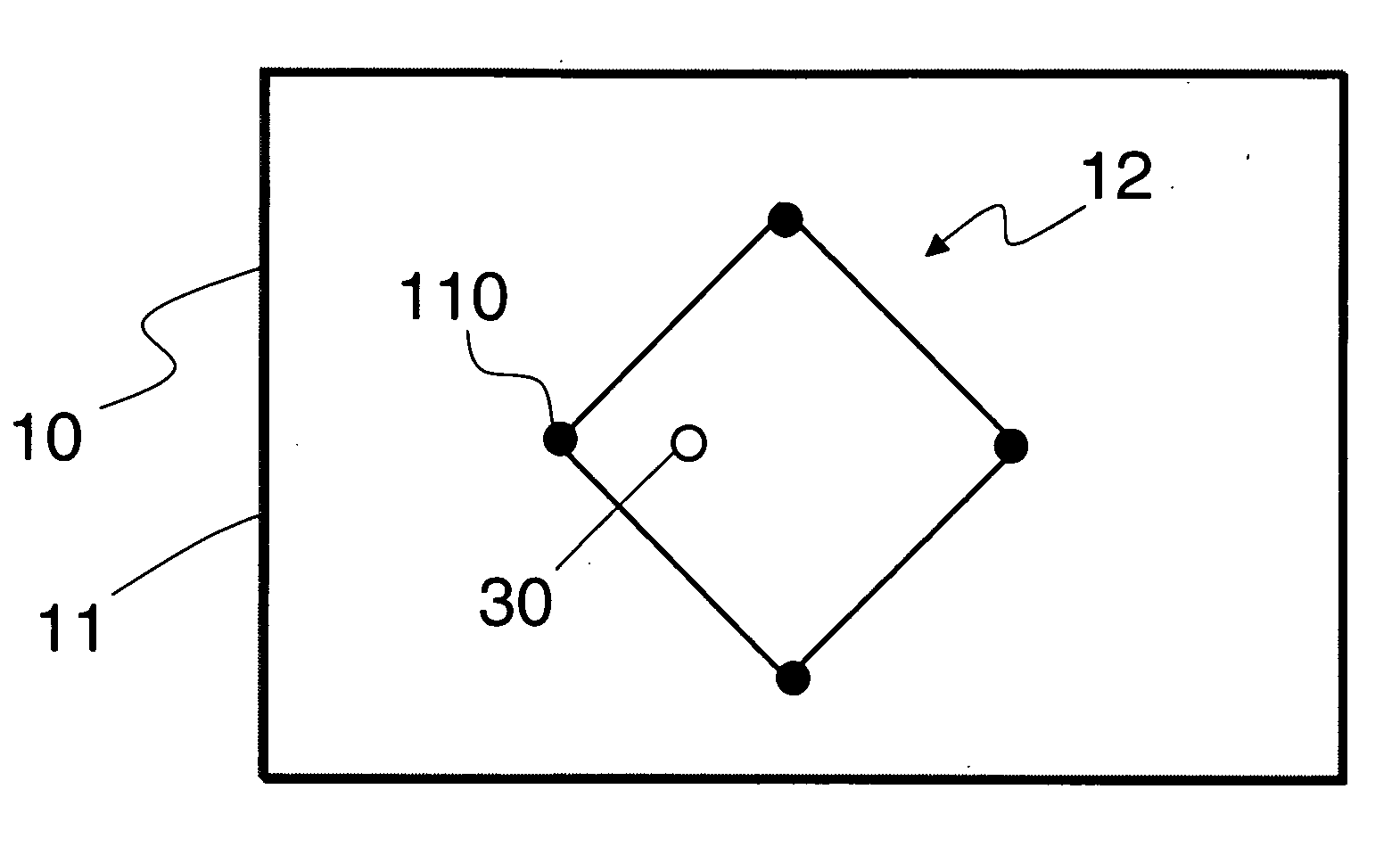
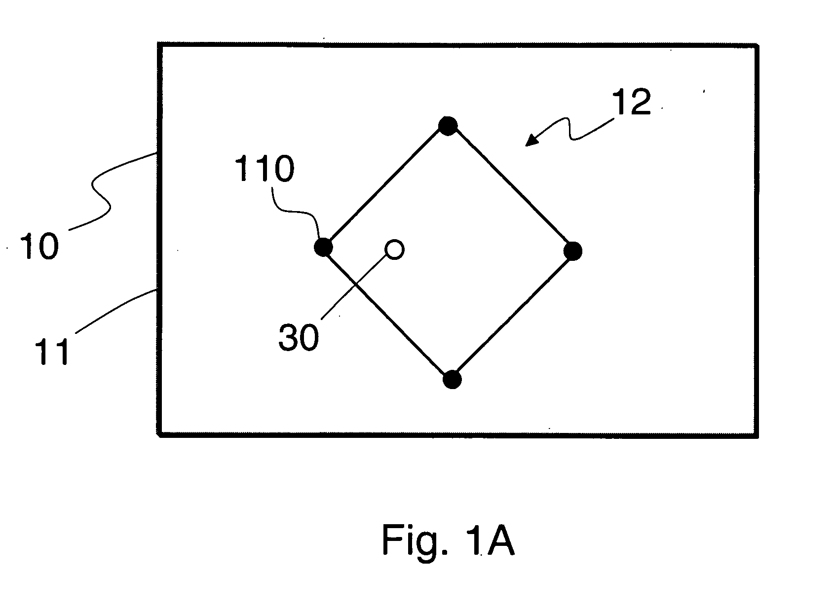
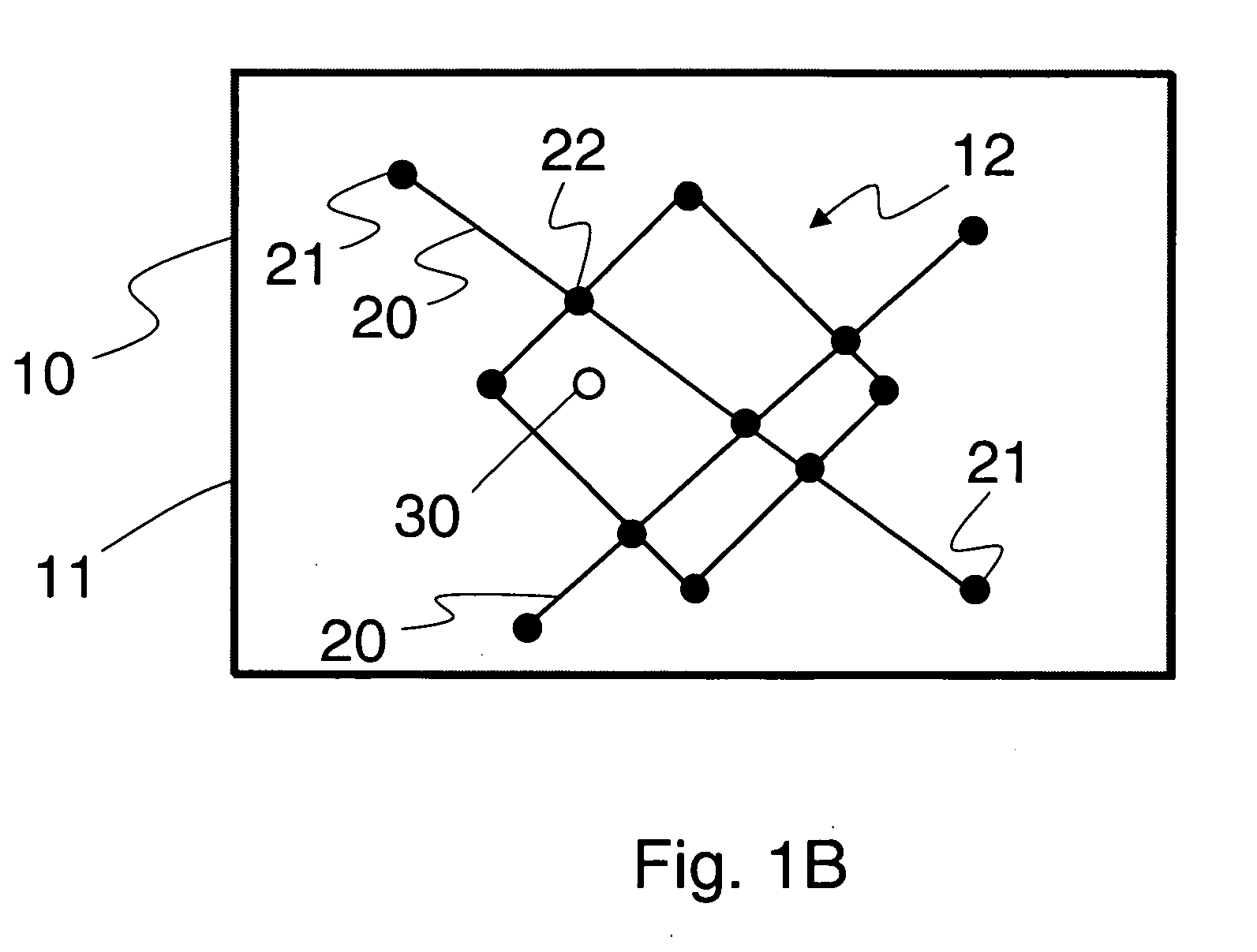
[0020]First, referring to FIG. 1A to FIG. 1E, which are views of a method for determining whether via hole on the printed circuit board is located within the geometric layout disclosed by the present invention. Shown in FIG. 1A is a printed circuit board 10 of the present invention which includes an edge 11 and on which is disposed with at least a geometric layout 12 and at least a via hole 30, wherein the geometric layout 12 is formed by connection of a plurality of vertex points 110. First, as shown in FIG. 1B, at least a line 20 is provided on the printed circuit board 10, each of the line 20 having two ends 21 and intersecting the geometric layout 12 to form a plurality of points of intersection 22. Then, as shown in FIG...


PUM


Abstract

A method for disposing power planes and ground planes of a printed circuit board (PCB), said method comprising the steps of: providing a PCB on which is disposed with a geometric layout and a via hole; providing a line on said PCB for intersecting said geometric layout to form a plurality of points of intersection; defining line segments by segmenting said line at each of said points of intersection to form a plurality of line segments; deleting some of said line segments having one end not being point of intersection for said geometric layout to form a plurality of segmented regions; searching a closed region by repeatedly searching region from any one of the points in said plurality of segmented regions; determining whether a closed region is a smallest closed region; determining whether a via hole is located within said smallest closed region.

Description

BACKGROUND OF THE INVENTION[0001]1. Field of the Invention[0002]The present invention is related to a method for disposing power planes and ground planes of printed circuit board, and more particularly, to a method of first segmenting the geometric layout into smallest closed region and then determining whether via hole on the printed circuit board is located in the smallest closed region.[0003]2. Description of the Prior Art[0004]Generally speaking, printed circuit boards are provided for electric components fixation and mechanical support, and for forming electric connection between electric components at the same time. Printed circuit boards are composed of insulation layer and conduction layer. The insulation layer is usually dielectric material that provides electric insulation between conduction layers. The conduction layer is patterned to form wiring to be used in the electric connection between electric components on the circuit board.[0005]In order to increase the function ...

Claims


Application Information

Patent Timeline
IPC IPC(8): G01B21/00G06F15/00
CPCH05K1/115H05K3/0005H05K1/0262H05K2201/09663H05K2201/093
Inventor TSAI, MING-CHIN
Owner KING YUAN ELECTRONICS
Why Eureka
Try Eureka