Storage electrode of a semiconductor device and method of forming the same

Active Publication Date: 2005-10-06
SAMSUNG ELECTRONICS CO LTD
View PDF4 Cites 1 Cited by
  • Summary
  • Abstract
  • Description
  • Claims
  • Application Information

AI Technical Summary

Benefits of technology

[0040] According to the embodiments of the present invention, storage electrodes may be spaced sufficiently far apart from each other so that a 2-bit

Problems solved by technology

However, as memory devices have become more highly integrated, forming a capacitor having a sufficient capacitance in a cell having very small area has become increasingly difficult.
According to the method of increasing the height of the capacitor, however, the higher a storage electrode is, the thicker a mold layer for a mold is required to be.
As a result, adjacent storage electrodes lean so that a 2-bit error between adjacent storage electrodes may be generated and also the leaning storage electrodes contact each other, thereby generating an electrical short between adja

Method used


Image

  • Storage electrode of a semiconductor device and method of forming the same
  • Storage electrode of a semiconductor device and method of forming the same
  • Storage electrode of a semiconductor device and method of forming the same

Examples


Example

First Embodiment

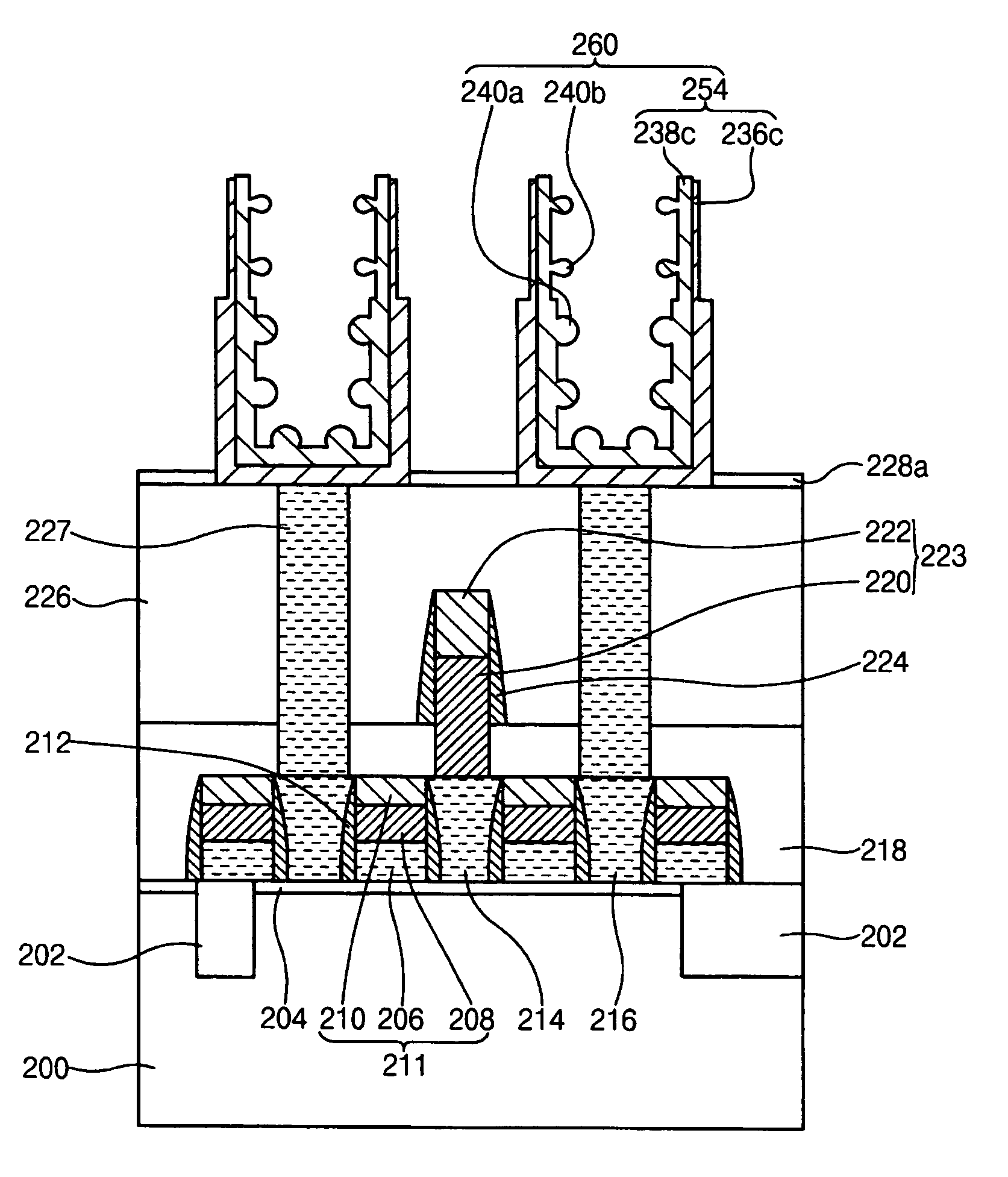
[0049]FIG. 1 illustrates a cross-sectional view of a storage electrode of a semiconductor device in accordance with a first embodiment of the present invention.

[0050] Referring to FIG. 1, a storage electrode 100 in accordance with the first embodiment includes a cylinder body 110 and a hemispherical silicon grain (HSG) layer 120. The cylinder body 110 includes an outer cylinder 130 and an inner cylinder 140 formed on inner surfaces of the outer cylinder 130. The HSG layer 120 is formed on inner surfaces of the inner cylinder 140.

[0051] The outer cylinder 130 may have a cylindrical shape having an open top and a closed bottom surface 132. The outer cylinder 130 may include a first outer cylindrical portion 134 having a first outer diameter A, and a second outer cylindrical portion 136 formed on the first outer cylindrical portion 136, the second outer cylindrical portion 136 having a second outer diameter B, which is less than the first outer diameter A. The first ...

Example

Second Embodiment

[0089]FIG. 11 illustrates a cross-sectional view of a storage electrode of a semiconductor device in accordance with a second embodiment of the present invention.

[0090] A storage electrode of the second embodiment includes elements substantially the same as those of the first embodiment as shown in FIG. 1 except with respect to a HSG layer. As noted above, like reference numerals and characters refer to substantially the same elements and dimensions as in FIG. 1, and detailed descriptions of the common elements and dimensions will not be repeated.

[0091] Referring to FIG. 11, a storage electrode 300 in accordance with the second embodiment includes the cylinder body 110 and a HSG layer 310. The cylinder body 110 includes the outer cylinder 130 and the inner cylinder 140 formed on inner surfaces of the outer cylinder 130. The HSG layer 310 is formed on the cylinder body 110.

[0092] The outer cylinder 130 may have a cylindrical shape having an open top and the close...


PUM


Abstract

In a storage electrode of a semiconductor device, and a method of forming the same, the storage electrode includes an outer cylinder including a first outer cylindrical portion having a first outer diameter, and a second outer cylindrical portion that is formed on the first outer cylindrical portion and having a second outer diameter, which is less than the first outer diameter, the first and second outer cylindrical portions having substantially equal inner diameters, and an inner cylinder formed on inner surfaces of the outer cylinder.

Description

BACKGROUND OF THE INVENTION [0001] 1. Field of the Invention [0002] The present invention relates to a storage electrode of a semiconductor device and a method of forming the storage electrode. More particularly, the present invention relates to a cylindrical storage electrode of a semiconductor memory device, e.g., a dynamic random access memory (DRAM) device, which is used for storing data, and a method of forming the storage electrode. [0003] 2. Description of the Related Art [0004] Generally, a semiconductor memory device, such as a DRAM device, stores information, e.g., data, program orders, and the like. The information may be read from the semiconductor memory device and other information may be additionally stored in the semiconductor memory device. The semiconductor memory device may include one transistor and one capacitor. [0005] The capacitor in the DRAM device may include a storage electrode, a dielectric layer and a plate electrode. To improve capacity of the memory de...

Claims


Application Information

Patent Timeline
IPC IPC(8): H01L21/02H01L21/20H01L21/8242H01L27/108
CPCH01L27/10814H01L27/10817H01L27/10852H01L28/84H01L28/90H10B12/318H10B12/315H10B12/033H10B12/00
Inventor KIM, KYOUNG-SEOKHWANG, KI-HYUNKIM, HYO-JUNGLEE, HYEON-DEOKNAM, SEOK-WOO
Owner SAMSUNG ELECTRONICS CO LTD
Why Eureka
Try Eureka