Process and Method for Logical-to-Physical Address Mapping in Solid Sate Disks

a technology of physical flash memory and process method, which is applied in the direction of memory address/allocation/relocation, instruments, computing, etc., can solve the problem that the fixed mapping of lbas to physical flash memory address is inadequate for managing data stored in such devices

Active Publication Date: 2010-02-04
INFINEON TECH AG
View PDF5 Cites 103 Cited by
  • Summary
  • Abstract
  • Description
  • Claims
  • Application Information

AI Technical Summary

Problems solved by technology

Due to the limitations of writing to flash memory devices described above wherein each write access requires a readout of an entire erase block, doing the erase and merging operations, and th

Method used


Image

  • Process and Method for Logical-to-Physical Address Mapping in Solid Sate Disks
  • Process and Method for Logical-to-Physical Address Mapping in Solid Sate Disks
  • Process and Method for Logical-to-Physical Address Mapping in Solid Sate Disks

Examples


Embodiment Construction

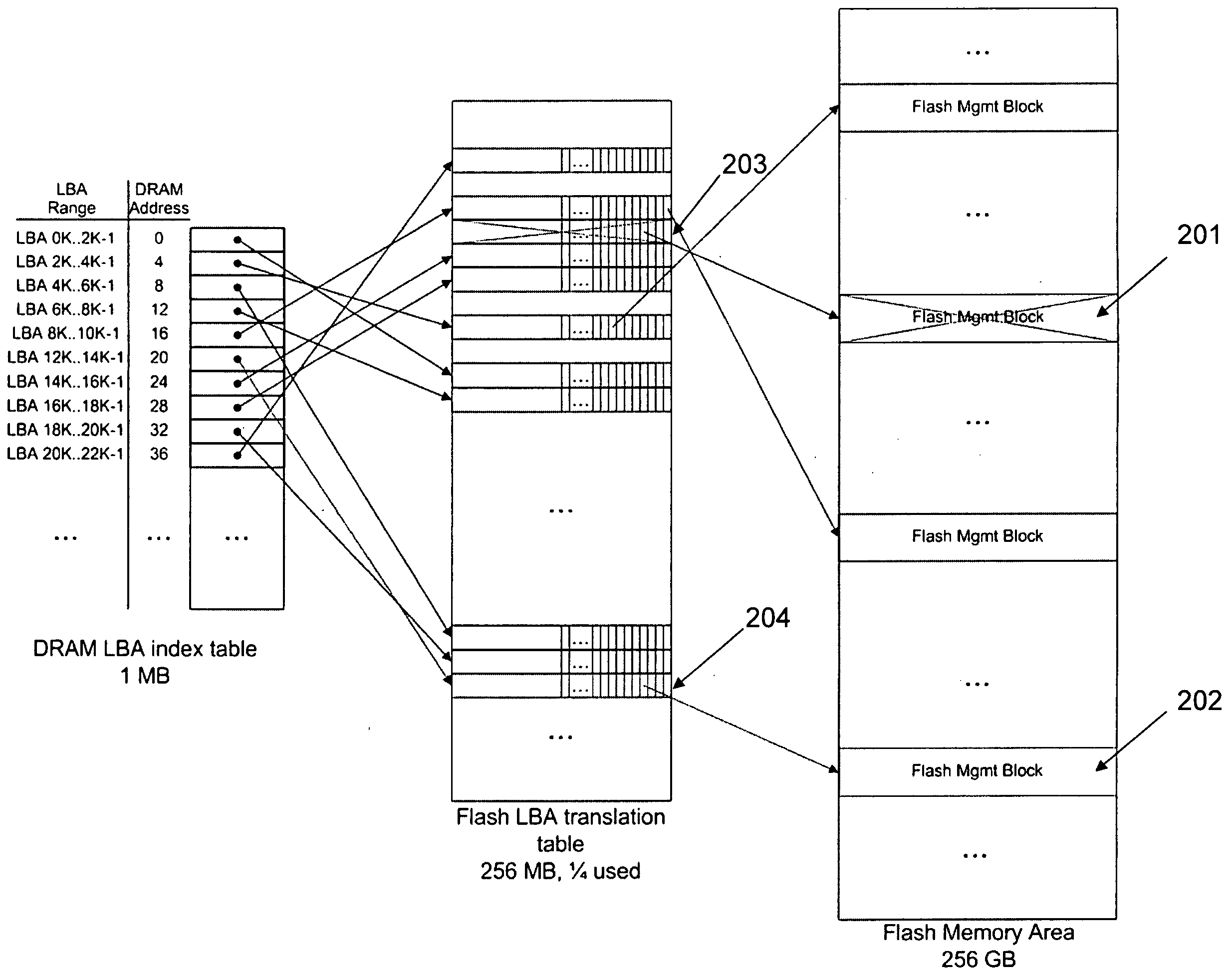
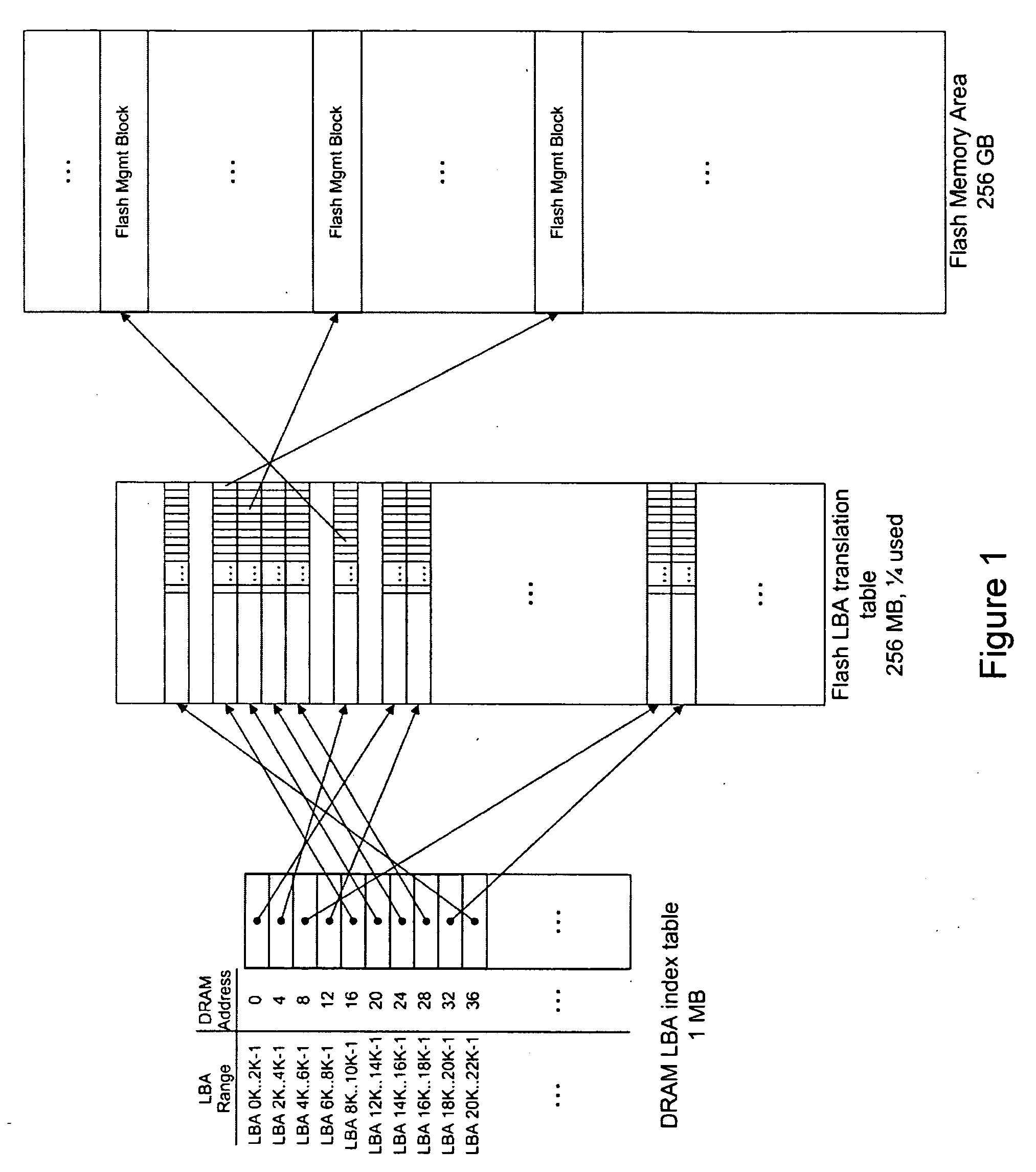
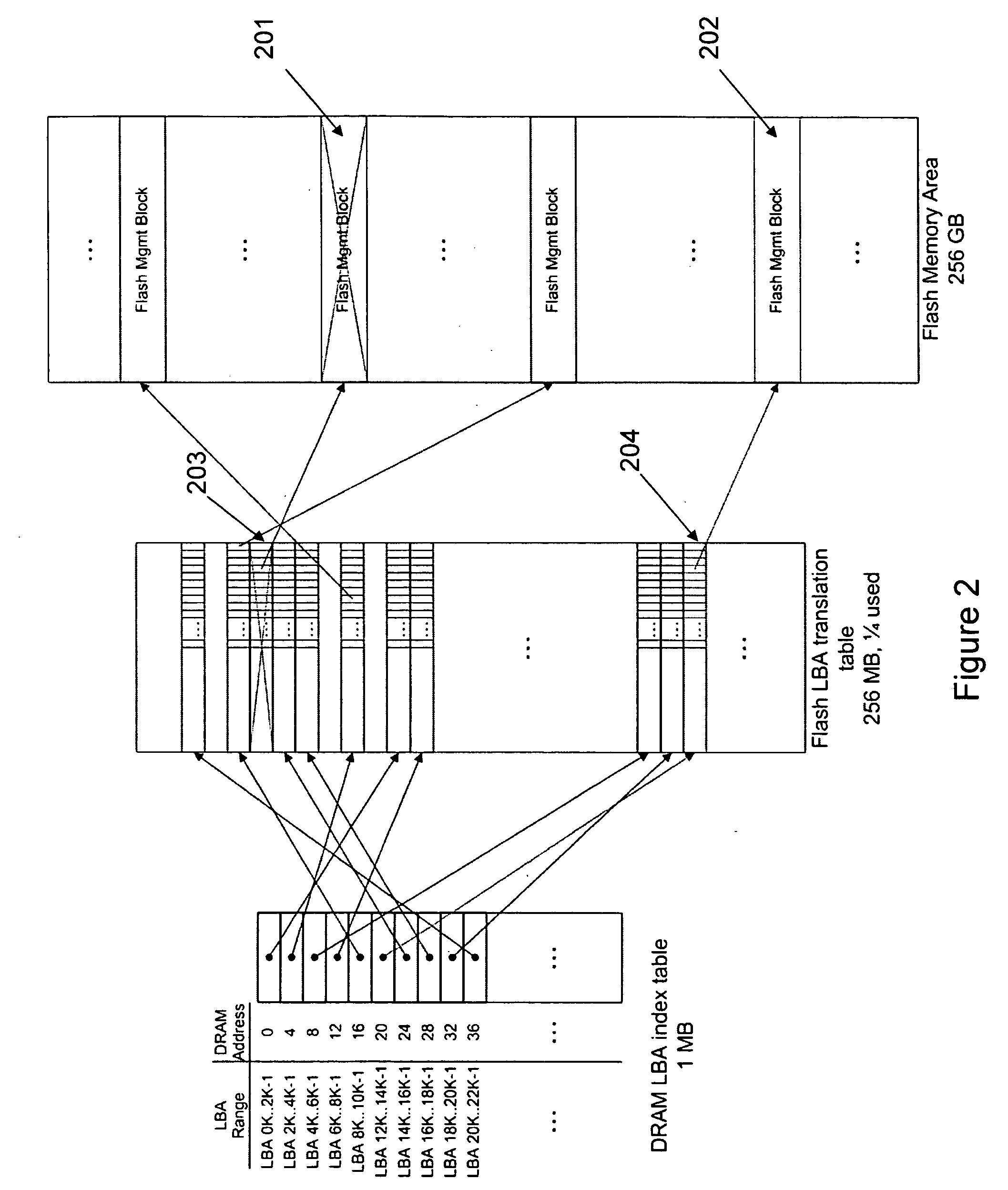
[0011]The making and using of the presently preferred embodiments are discussed in detail below. It should be appreciated, however, that the present invention provides many applicable inventive concepts that can be embodied in a wide variety of specific contexts. The specific embodiments discussed are merely illustrative of specific ways to make and use the invention, and do not limit the scope of the invention.

[0012]The present invention will be described with respect to exemplary embodiments in a specific context, namely a mass storage device including a volatile memory device and a nonvolatile memory device to provide a nonvolatile memory device with improved storage performance.

[0013]An embodiment of the invention may be applied to a mass storage device, for example, to a solid-state drive formed with a flash memory device. Other mass storage devices can be constructed that include a memory device that can be readily overwritten with a nonvolatile memory device as introduced her...


PUM


Abstract

An embodiment of the invention relates to a mass storage device including a nonvolatile memory device with a plurality of memory management blocks and an address translation table formed with pointers to locations of the memory management blocks. A volatile memory device is included with an address index table formed with pointers to the pointers to the locations of the memory management blocks. The address index table is stored in the nonvolatile memory upon loss of bias voltage. Changes to the address translation table are accumulated in the volatile memory and written to the address translation table when at least a minimum quantity of the changes has been accumulated. The changes to the logical block address translation table accumulated in the volatile memory are written to a page in the address translation table after prior data in the page has been updated, written to another page, and then erased.

Description

TECHNICAL FIELD[0001]An embodiment of the invention relates generally to mass storage devices and methods, and more particularly to combining a nonvolatile memory device with a memory device that can be more easily overwritten to provide a nonvolatile memory device with improved access to and storage of digital data.BACKGROUND[0002]Mass storage memory devices such as flash cards, USB (“universal serial bus”) sticks, or solid-state disks use flash semiconductor structures to store data in a nonvolatile memory device. A nonvolatile memory device refers to a memory device for which a power source can be switched “off” without losing the contents of the memory. Nonvolatile memory devices include flash memory devices that may semi-permanently retain an electric charge to represent one or more bits, or a “hard disk” (also referred to as a “hard drive”) that may a semi-permanently retain a magnetic charge to store one or more bits. Semiconductor devices such as SRAMs (static random access ...

Claims


Application Information

Patent Timeline
IPC IPC(8): G06F12/00
CPCG06F12/0246G06F2212/7201G06F2212/1032G06F2212/1016G06F3/061G06F3/0616G06F3/064G06F3/0679
Inventor HINZ, TORSTEN
Owner INFINEON TECH AG
Why Eureka
Try Eureka