Thin-film transistor substrate and method of fabricating the same

a thin film transistor and substrate technology, applied in the direction of transistors, electrical equipment, semiconductor devices, etc., can solve the problems of increasing time and cost required to fabricate each signal delivery line, and achieve the effect of reducing cost and simple fabrication

Inactive Publication Date: 2010-02-11
SAMSUNG DISPLAY CO LTD
View PDF3 Cites 11 Cited by
  • Summary
  • Abstract
  • Description
  • Claims
  • Application Information

AI Technical Summary

Benefits of technology

[0008]The present invention provides a thin-film transistor (TFT) substrate that can be fabricated simply and at reduced cost.

Problems solved by technology

However, as the number of layers that form each signal delivery line increases, the time and cost required to fabricate each signal delivery line also increases.

Method used


Image

  • Thin-film transistor substrate and method of fabricating the same
  • Thin-film transistor substrate and method of fabricating the same
  • Thin-film transistor substrate and method of fabricating the same

Examples


Embodiment Construction

, Experimental Example 2, and Experimental Example 3 of Table 1 were conducted.

[0019]FIG. 12B shows an AFM image of the top surface of the data wiring at a location where Experimental Example 4, Experimental Example 5, and Experimental Example 6 of Table 1 were conducted.

[0020]FIG. 13A shows an AFM image of a top surface of data wiring at a location where Comparative Experimental Examples 1, Comparative Experimental Example 2, and Comparative Experimental Example 3 of Table 1 were conducted.

[0021]FIG. 13B shows an AFM image of the top surface of the data wiring at a location where Comparative Experimental Example 4, Comparative Experimental Example 5, and Comparative Experimental Example 6 of Table 1 were conducted.

DETAILED DESCRIPTION OF THE ILLUSTRATED EMBODIMENTS

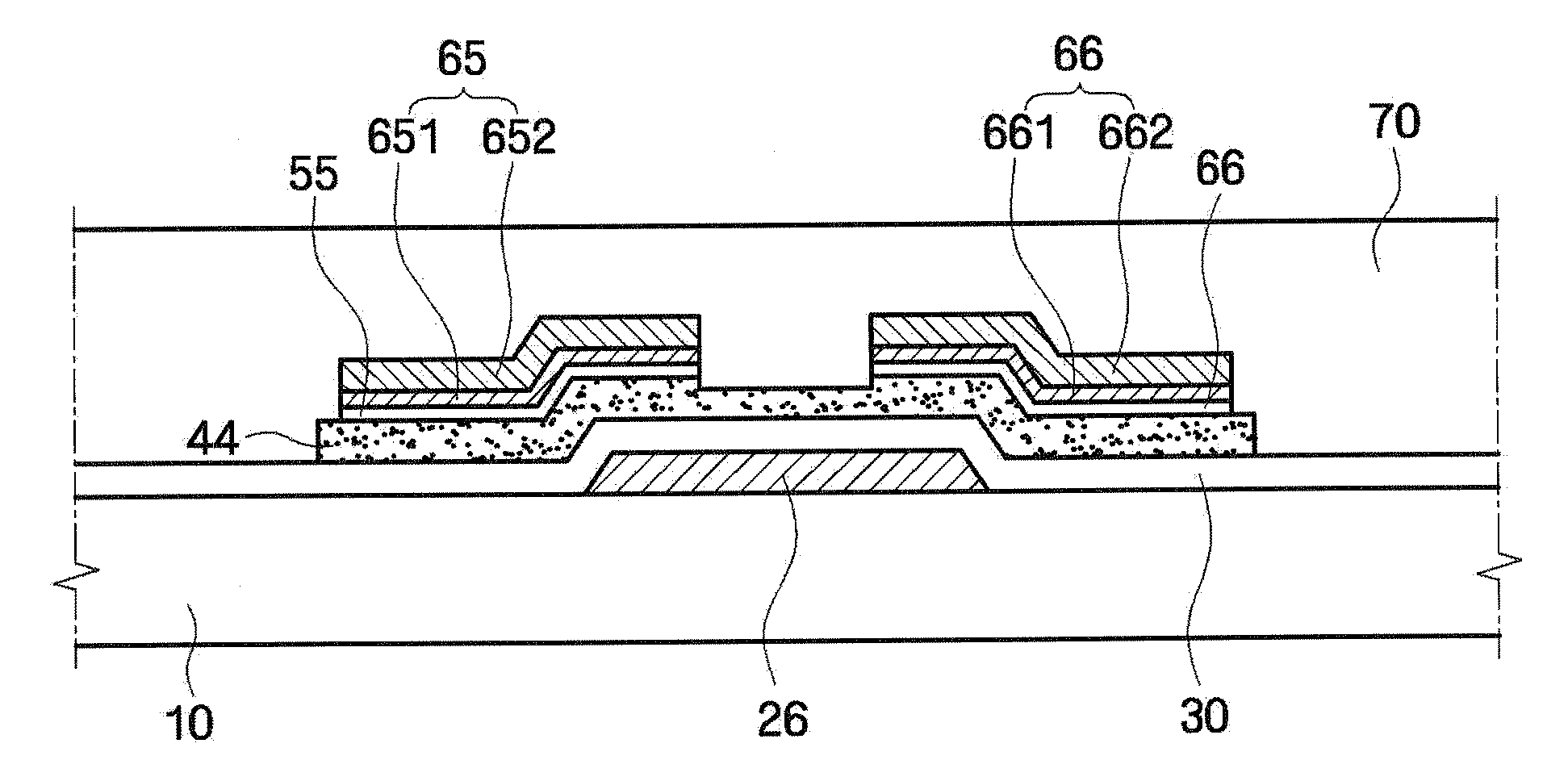
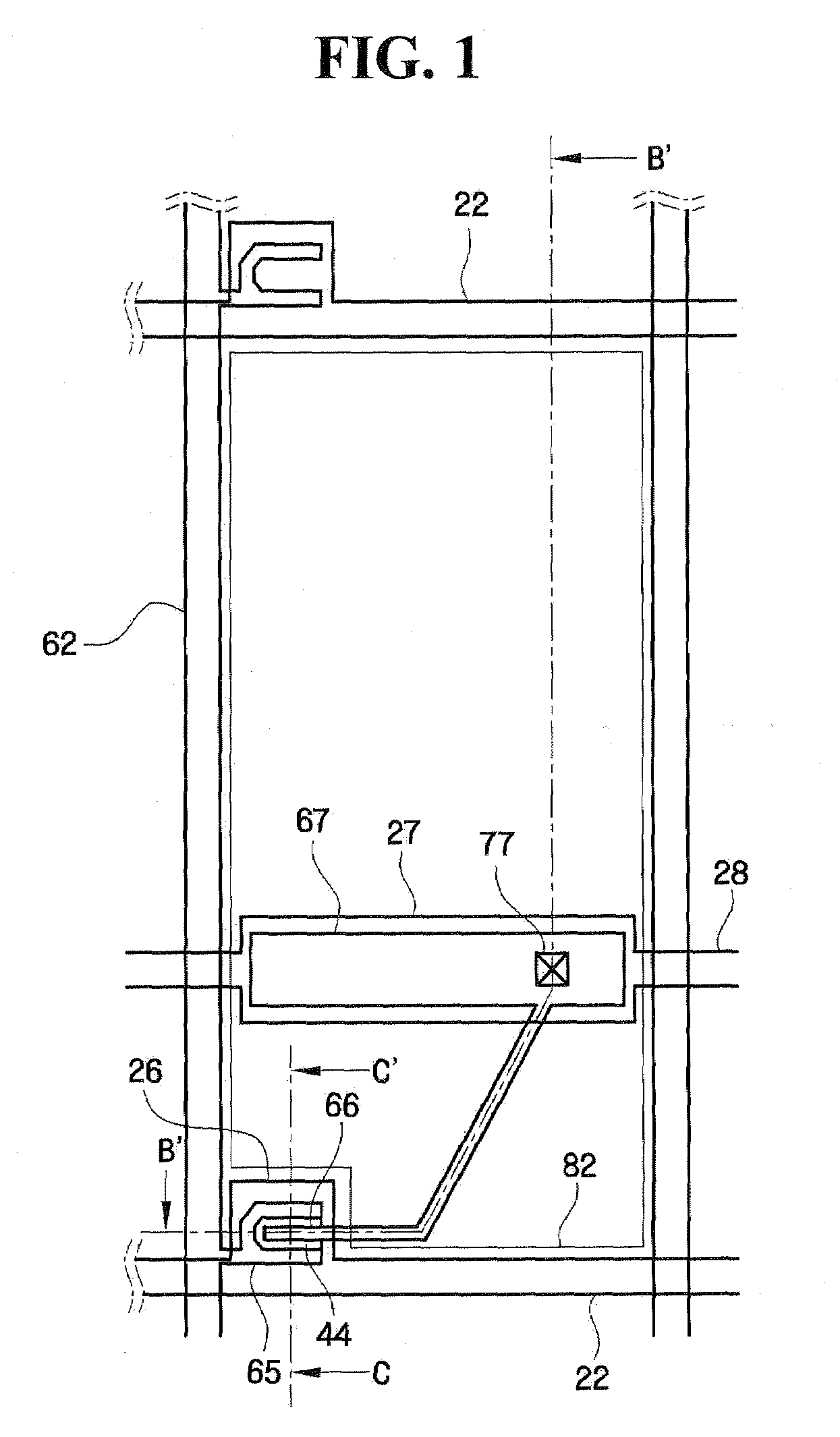
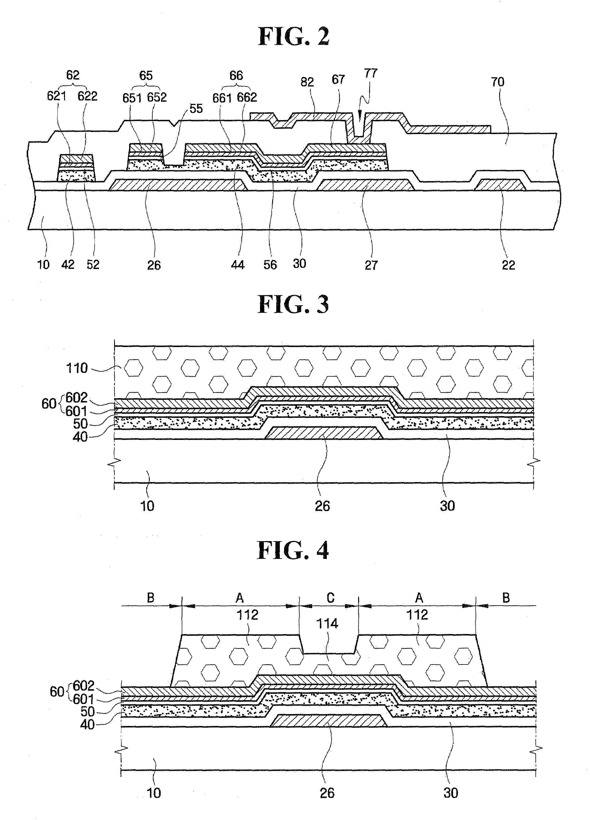
[0022]The invention is described more fully hereinafter with reference to the accompanying drawings, in which exemplary embodiments of the invention are shown. This invention may, however, be embodied in many different fo...


PUM


Abstract

The present invention provides a thin-film transistor (TFT) substrate, which can be fabricated simply and at reduced cost, and a method of fabricating the TFT substrate. The TFT substrate includes: an insulating substrate; gate wiring that extends on the insulating substrate in a first direction; data wiring that extends on the gate wiring in a second direction, and includes a lower layer and an upper layer; and a semiconductor pattern that is disposed under the data wiring and has substantially the same shape as the data wiring except for a channel region, wherein root-mean-square roughness of a top surface of the data wiring is 3 nm or less.

Description

[0001]This application claims priority from and the benefit of Korean Patent Application No. 10-2008-0078154, filed on Aug. 8, 2008, which is hereby incorporated by reference for all purposes as if fully set forth herein.BACKGROUND OF THE INVENTION[0002]1. Field of the Invention[0003]The present invention relates to a thin-film transistor (TFT) substrate and a method of fabricating the same, and more particularly, to a TFT substrate, which can be fabricated simply and at reduced cost, and a method of fabricating wiring of the TFT substrate.[0004]2. Discussion of the Background[0005]Liquid crystal displays (LCDs) are one of the most widely used flat panel displays. An LCD may include two substrates having electrodes formed thereon and a liquid crystal layer disposed between the two substrates. The LCD applies voltages to the electrodes to rearrange liquid crystal molecules of the liquid crystal layer, and thus control the amount of light that passes through the liquid crystal layer.[...

Claims


Application Information

Patent Timeline
Patent Type & Authority Applications(United States)
IPC IPC(8): H01L29/786H01L21/20
CPCH01L29/458H01L27/1288H01L27/124
Inventor CHOI, SEUNG-HAKIM, SANG-GABCHOI, SHIN-IILEE, KI-YEUPYANG, DONG-JUCHIN, HONG-KEEJEONG, YU-GWANG
Owner SAMSUNG DISPLAY CO LTD
Why Eureka
Try Eureka