Active matrix substrate, liquid crystal display panel, liquid crystal display element, liquid crystal display device, and substrate for liquid crystal display panels

Active Publication Date: 2010-02-25
SHARP KK
View PDF17 Cites 23 Cited by
  • Summary
  • Abstract
  • Description
  • Claims
  • Application Information

AI Technical Summary

Benefits of technology

[0084]It is preferable that the liquid crystal display device is a television receiver. In a field of the television receiver, a high display quality is now being furthermore demanded along with spread of high-definition television broadcasting and an increase in screen size. The liquid crystal display device of the present invention can provide high display qualities, and therefore a high-quality television receiver can be provided. In the present description, the “television receiver” means a receiver with which a viewer receives television broadcasting and views displayed images. The television receiver generally has a built-in tuner, but the liquid crystal display device of the present invention may be a monitor which has no built-in tuner.
[0085]The present invention is a substrate for liquid crystal display panels, including a third spacer on a substrate, wherein the third spacer includes a third base layer and a covering layer, the third base layer having a thickness of submicron order, the third base layer being buried in the covering layer. According to this, the third base layer pushes u

Problems solved by technology

Therefore, sufficient flatness can not be secured in certain instances.
As a result, the cell gap becomes uneven.
However, only a few materials can secure it, generally.
Therefore, there is room for improvement in that a degree of freedom of material selection is low, which affects

Method used


Image

  • Active matrix substrate, liquid crystal display panel, liquid crystal display element, liquid crystal display device, and substrate for liquid crystal display panels
  • Active matrix substrate, liquid crystal display panel, liquid crystal display element, liquid crystal display device, and substrate for liquid crystal display panels
  • Active matrix substrate, liquid crystal display panel, liquid crystal display element, liquid crystal display device, and substrate for liquid crystal display panels

Examples


embodiment 1

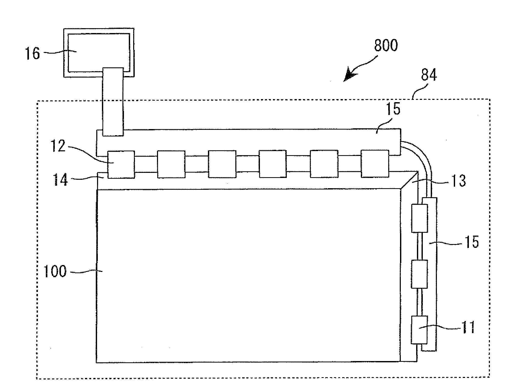
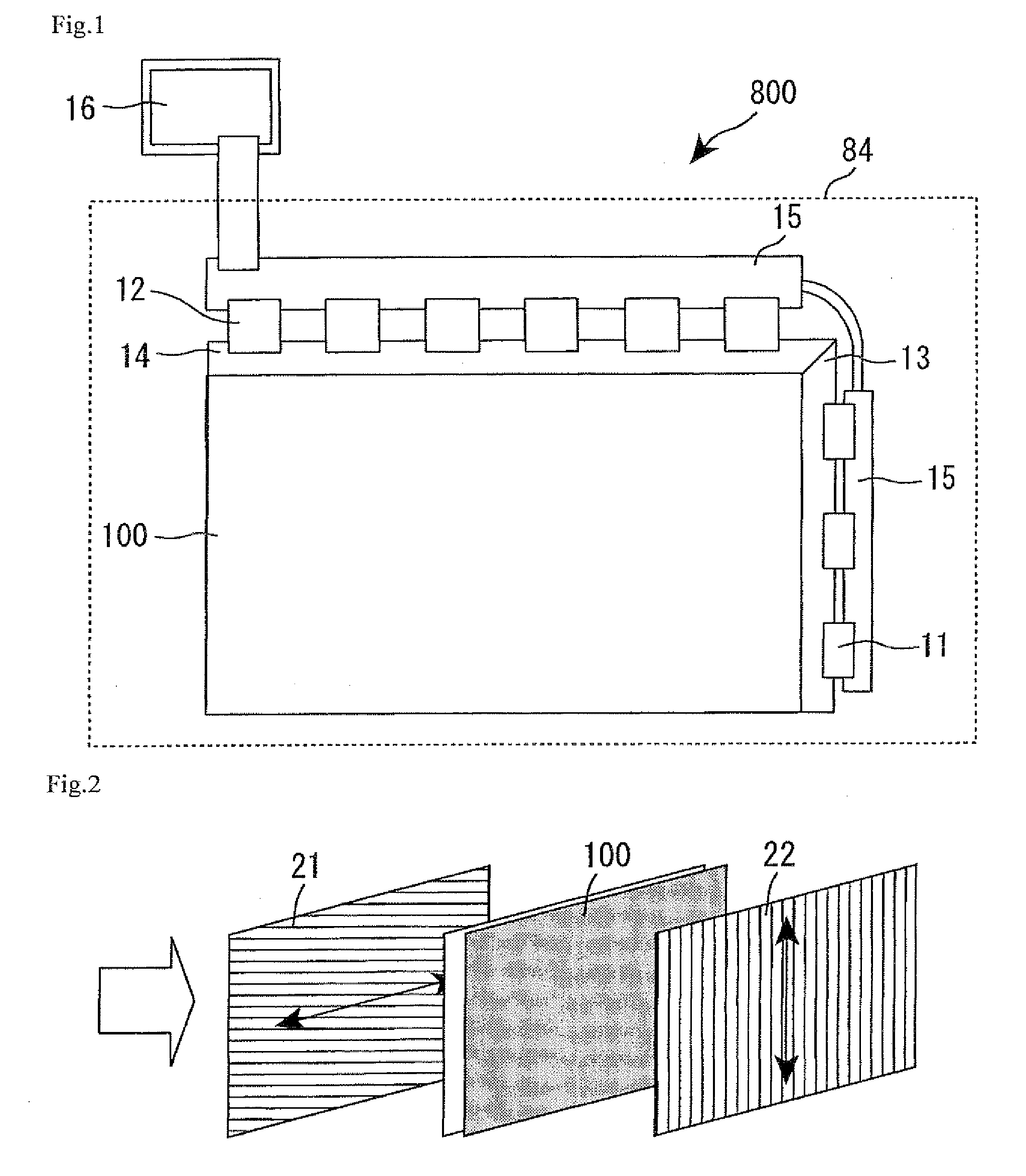
[0120]FIG. 1 is a planar view schematically showing a configuration of a liquid crystal display device in Embodiment 1.

[0121]The liquid crystal display device in the present Embodiment includes a liquid crystal display element 84, a display control circuit 16, and a backlight (not shown), as shown in FIG. 1. The liquid crystal display element 84 includes a liquid crystal display panel 100, a gate driver 11, a source driver 12, a gate terminal part 13, a source terminal part 14, and a printed wire board (PWB) 15. The liquid crystal display panel 100 includes an active matrix substrate and a color filter substrate, and on the back surface side and the observation surface side, a polarizer is attached.

[0122]FIG. 2 is a perspective view schematically showing arrangement relationship among a liquid crystal display panel and two polarizers attached thereto. The double arrows in the polarizers 21 and 22 show an axis direction of a polarization axis of each polarizer. The outline arrow show...

embodiment 2

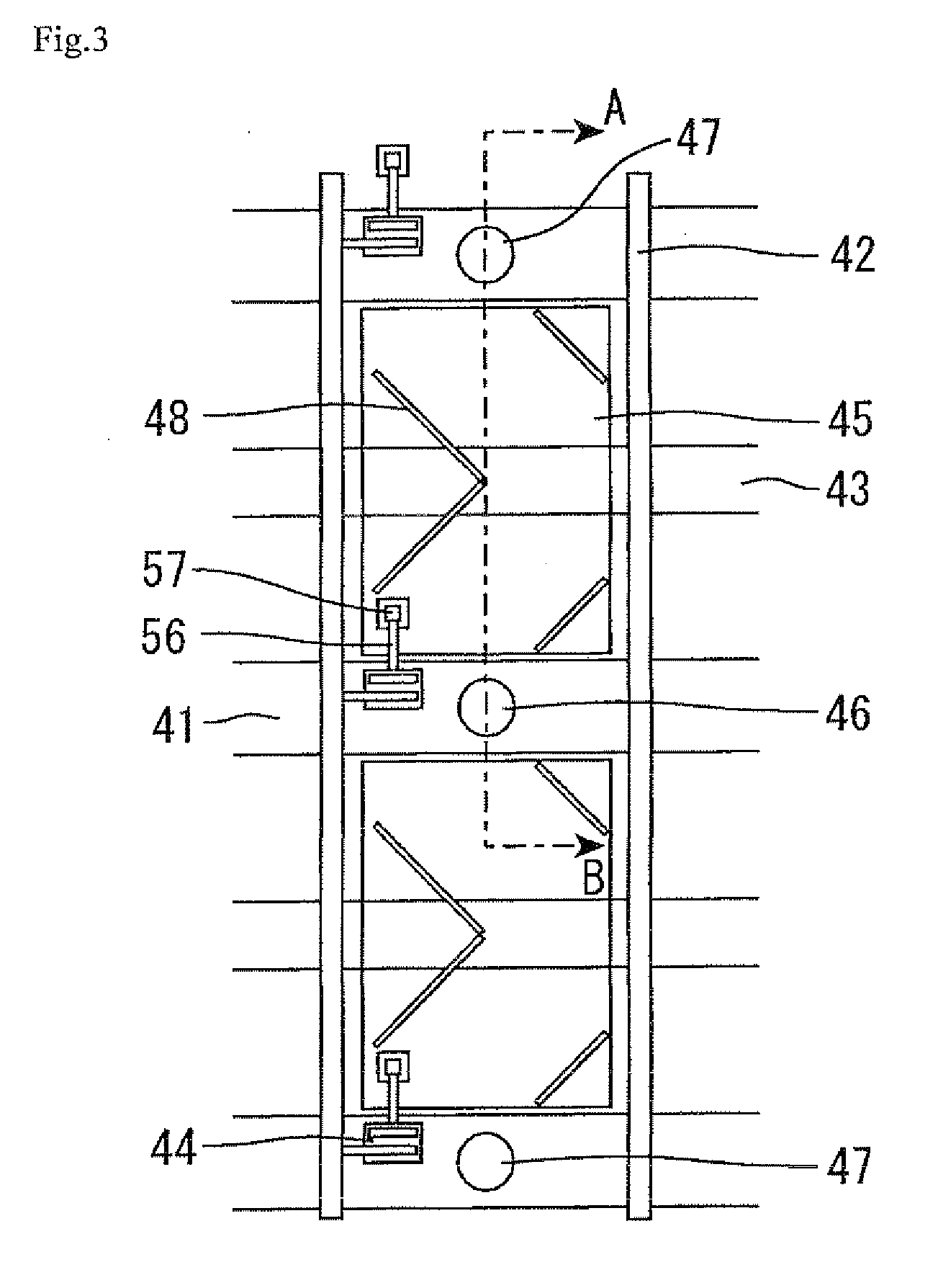
[0183]FIG. 13 is a planar view schematically showing a configuration of an active matrix substrate included in a liquid crystal display device in accordance with Embodiment 2.

[0184]The liquid crystal display device in the present Embodiment has the same configuration as in Embodiment 1, except for the configuration of the active matrix substrate. Specifically, according to Embodiment 1, as shown in FIG. 3, the pixel electrode 45 is provided with the alignment control slit 48 for controlling alignment of liquid crystal. According to Embodiment 2, an alignment control projection 49 is arranged on the pixel electrode 45, as shown in FIG. 13. The alignment control projection 49 is formed simultaneously with the resin layer 63 of the first spacer 46 and the second spacer 47. Therefore, the production steps are not increased.

[0185]Embodiments other than the configuration and the production method of the active matrix substrate are omitted because they are the same as in Embodiment 1.

embodiment 3

[0186]FIG. 14 is a planar view schematically showing a configuration of an active matrix substrate included in a liquid crystal display panel in accordance with Embodiment 3.

[0187]FIG. 15 is a planar view schematically showing a configuration of a color filter substrate included in a liquid crystal display panel in accordance with Embodiment 3.

[0188]FIG. 16 is a cross-sectional view schematically showing the color filter substrate taken along line A-B in FIG. 15.

[0189]The liquid crystal display panel in accordance with the present Embodiment includes column spacers 96 and 97 not on the active matrix substrate 1 but on the color filter substrate (substrate for liquid crystal display panels) 2, as shown in FIGS. 14 to 16.

[0190]The third spacer 96 is composed of the third dotted base layer 91 and a resin layer (the third covering layer) 98 in which the third base layer 91 is buried. Further, the top of the third spacer 96 is flat. The third base layer 91 is composed of the same metal m...


PUM


Abstract

The present invention has an object to provide an active matrix substrate, a liquid crystal display panel, a liquid crystal display element, a liquid crystal display device, and a substrate for liquid crystal display panel, each capable of suppressing generation of uneven cell gap without increase in a parasitic capacitance of a wiring. The active matrix substrate of the present invention is an active matrix substrate including a spacer on a substrate, wherein the spacer includes a base layer and a covering layer, the base layer being buried in the covering layer.

Description

TECHNICAL FIELD[0001]The present invention relates to an active matrix substrate, a liquid crystal display panel, a liquid crystal display element, a liquid crystal display device, and a substrate for liquid crystal display panels. More specifically, the present invention relates to an active matrix substrate, a liquid crystal display panel, a liquid crystal display element, a liquid crystal display device, and a substrate for liquid crystal display panels, each including a spacer on a substrate.BACKGROUND ART[0002]A color liquid crystal display device which is currently widely used includes a color filter arranged in a sub-pixel (dot). Color filters of three primary colors of light, i.e., red (R), green (G), and blue (B), are arranged in sub-pixels in a specific pattern, typically. Thus, according to the color liquid crystal display device, one pixel is composed of three sub-pixels of R, G, and B. This pixel serves as the minimum constitutional unit of a screen to provide color dis...

Claims


Application Information

Patent Timeline
IPC IPC(8): G02F1/1333G02F1/1339
CPCG02F1/13394G02F2001/13398G02F2001/13396G02F1/13396G02F1/13398
Inventor TOKUDA, TSUYOSHIAKIYAMA, HIROTOSHORAKU, AKIHIROTSUBATA, TOSHIHIDEKUROZUMI, YUKIO
Owner SHARP KK
Why Eureka
Try Eureka