Semiconductor structure and method of manufacture of same

a technology of semiconductors and semiconductors, applied in the direction of crystal growth process, after-treatment details, polycrystalline material growth, etc., can solve the problems of high quality, difficult to achieve zincblende (algain)n substrates, and inability to commercially exist,

Inactive Publication Date: 2010-03-04
SHARP KK
View PDF3 Cites 17 Cited by
  • Summary
  • Abstract
  • Description
  • Claims
  • Application Information

AI Technical Summary

Problems solved by technology

However, high quality zincblende (AlGaIn)N substrates are difficult to achieve and are not commercially available at present.
However, the method of Yang et al. is undesirable as it did not produce zincblende GaN with suitable high optical quality.
This is likely to be due to poor crystal quality through the use of plasma assisted MBE, which is a low temperature method, for the final GaN layer and not using arsenic or phosphorus mediated GaN epitaxy for initial growth on the GaAs layer.
This method is undesirable for zincblende (AlGaIn)N because of the difficulties associated with depositing boron phosphide, such as precursor toxicity.
Also this deposition technique is limited to a vapour phase method such as MOVPE.
Also, the method of Zhao et al. resulted in poor crystal quality and optical properties were not reported.

Method used


Image

  • Semiconductor structure and method of manufacture of same
  • Semiconductor structure and method of manufacture of same

Examples


example

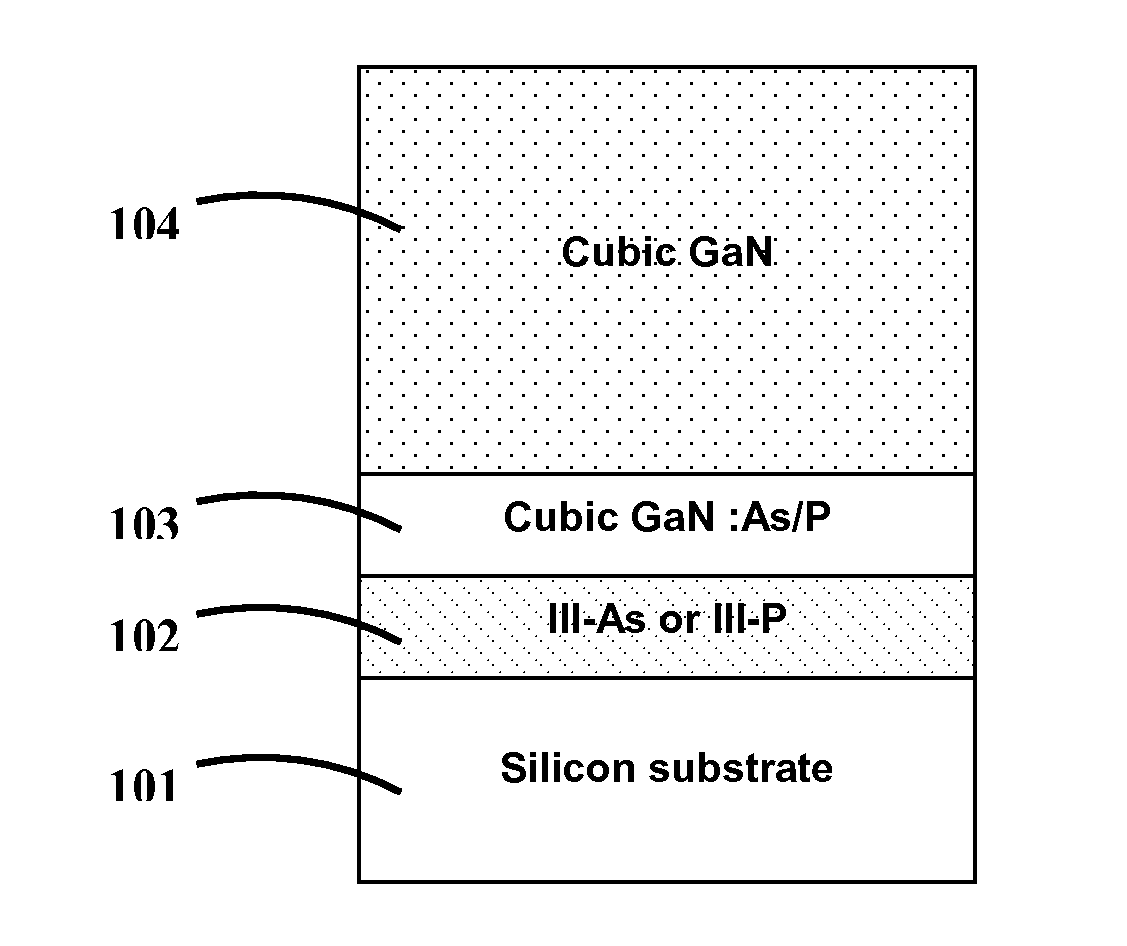
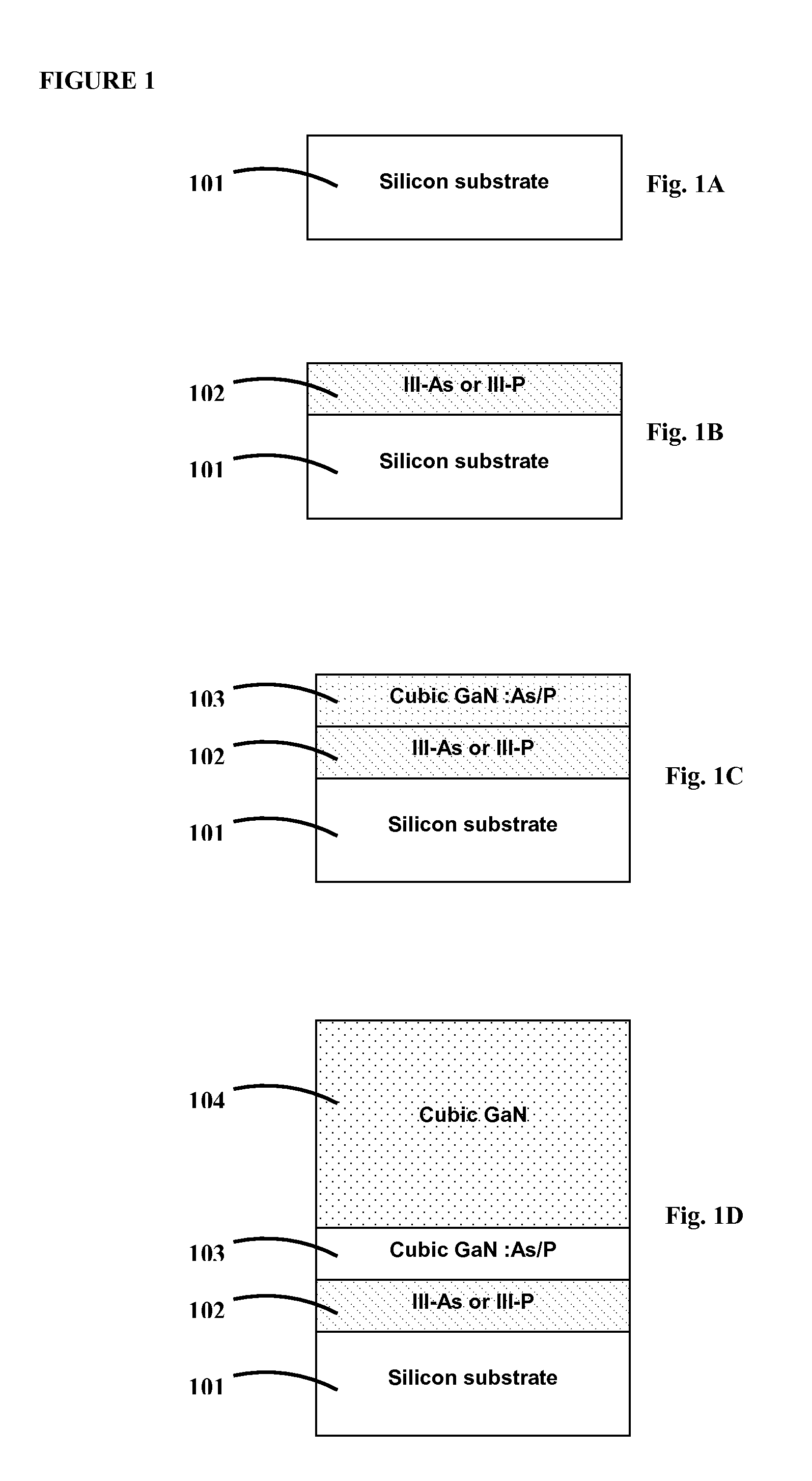
[0044]As a particular example of the method and structure in accordance with the present invention, FIG. 1A illustrates a clean silicon substrate 101 that is loaded into the MBE chamber and heat treated under vacuum to remove surface oxides. A typical heat treatment is 1000° C. for 15 minutes duration. The silicon substrate 101 is then cooled under vacuum prior to carrying out the following stages:

Stage 1: AlInGaAs Deposition

[0045]FIG. 1B shows a 50 nm thick layer of AlInGaAs 102 that is deposited onto the silicon substrate 101 at a temperature of 400° C. More generally, the AlInGaAs layer 102 more preferably has a thickness in the range 10 nm to 100 nm and may be grown at a temperature in the range 250° C. to 500° C., for example. Arsenic-rich conditions are used.

[0046]The thin layer 102 is desirable to allow re-crystalisation during Stage 2. The low growth temperature is desirable to achieve full surface coverage and trapping of defects / dislocations during Stage 2.

[0047]Coating th...


PUM


Abstract

A method of manufacturing a nitride semiconductor structure includes disposing a semiconductor substrate in a molecular beam epitaxy reactor; growing a wetting layer comprising AlxInyGa(1−(x/y))As(0≦x+y≦1) or AlxInyGa(1−(x/y))P(0≦x+y≦1) on the substrate; in-situ annealing the wetting layer; growing a first AlGaInN layer on the wetting layer using plasma activated nitrogen as the source of nitrogen with an additional flux of phosphorous or arsenic; and growing a second AlGaInN layer on the first AlGaInN layer using ammonia as a source of nitrogen.

Description

TECHNICAL FIELD [0001]The present invention relates to a semiconductor structure, and in particular to a semiconductor structure with a zincblende crystal structure fabricated in a nitride materials system such as, for example, the (Al,Ga,Tn)N materials system. The present invention also relates to a method of manufacture of a zincblende semiconductor structure, and in particular to manufacture of a zincblende semiconductor structure in a nitride materials system such as, for example, the (Al,Ga,Tn)N materials system. The invention may also be applied to a substrate for the manufacture of an optoelectronic semiconductor device such as a light emitting diode (LED) or laser diode (LD), or an electronic semiconductor device such as a heterostructure field effect transistor (HFET) or a high electron mobility transistor (HEMT).BACKGROUND OF THE INVENTION [0002]Plasma assisted molecular beam epitaxy (MBE) is the deposition of a III-V semiconductor by MBE where the group V source (for exam...

Claims


Application Information

Patent Timeline
Patent Type & Authority Applications(United States)
IPC IPC(8): H01L29/205H01L21/205
CPCC30B23/02C30B25/02C30B29/40C30B29/403C30B33/02H01L21/02381H01L29/2003H01L21/02461H01L21/02463H01L21/02502H01L21/0254H01L21/02631H01L21/02458
Inventor HOOPER, STEWART EDWARDHEFFERNAN, JONATHAN
Owner SHARP KK
Why Eureka
Try Eureka