Method of driving pixel circuit, light emitting device, and electronic apparatus

Active Publication Date: 2010-03-04
SEIKO EPSON CORP
View PDF17 Cites 28 Cited by
  • Summary
  • Abstract
  • Description
  • Claims
  • Application Information

AI Technical Summary

Benefits of technology

[0007]According to a first aspect of the invention, there is provided a method of driving a pixel circuit that includes: a light emitting element; a driving transistor that is connected to the light emitting element in series; and a storage capacitor that is interposed between a path, which is formed between the light emitting element and the driving transistor, and a gate of the driving transistor. The method includes: having a voltage between both ends of the storage capacitor gradually approach a threshold voltage of the driving transistor for a compensation period as a first compensation operation for a compensation period by having the driving transistor to be in the conductive state and supplying a reference electric potential (for example, the reference electric potential VREF) to the gate of the driving transistor; changing the electric potential of the gate of the driving transistor in accordance with a gray scale electric potential according to a gray scale value designated to the pixel circuit and having the voltage between both ends of the storage capacitor gradually approach the threshold voltage of the driving transistor over a temporal length (for example, a temporal length tb) that is set to be changed in accordance with the gray scale value for a write period after the elapse of the compensation period as a second compensation operation; and supplying a driving current according to the voltage between the both ends of the storage capacitor to the light emitting element by stopping supply of the electric potential to the gate of the driving transistor for a driving period after elapse of the write period. According to the above-described driving method, the temporal length of the second compensation operation is set to be changed in accordance with the gray scale value (or the gray scale electric potential). Accordingly, it is possible to effectively suppress the error in the driving current for a plurality of the gray scale values.
[0045]According to the light emitting device of the sixth aspect, the same advantages as those of the driving method according to the sixth aspect are acquired.

Problems solved by technology

Light emitting devices in which a driving transistor controls the amount of a driving current supplied to a light emitting element suffer from errors (deviations from a target value or non-uniformity between elements) in the electrical characteristics of the driving transistors or the light emitting elements.
Therefore, errors in the driving current in some gray scale values may not be removed.
Thus, there are cases where the error in the driving current cannot be eliminated depending on the gray scale value.
However, under the tendency that the temporal length of the second compensation operation, for which the error in the driving current is suppressed, is lengthened as the gray scale value is smaller, in order to minimize the error in the driving current even for a case where the gray scale value is small, an excessively long temporal length needs to be acquired for the second compensation operation.
However, under the tendency that the temporal length of the second compensation operation, for which the error in the driving current is suppressed, is lengthened as the gray scale value is smaller, in order to minimize the error in the driving current even for a case where the gray scale value is small, an excessively long temporal length needs to be acquired for the operation.

Method used


Image

  • Method of driving pixel circuit, light emitting device, and electronic apparatus
  • Method of driving pixel circuit, light emitting device, and electronic apparatus
  • Method of driving pixel circuit, light emitting device, and electronic apparatus

Examples


first embodiment

A: FIRST EMBODIMENT

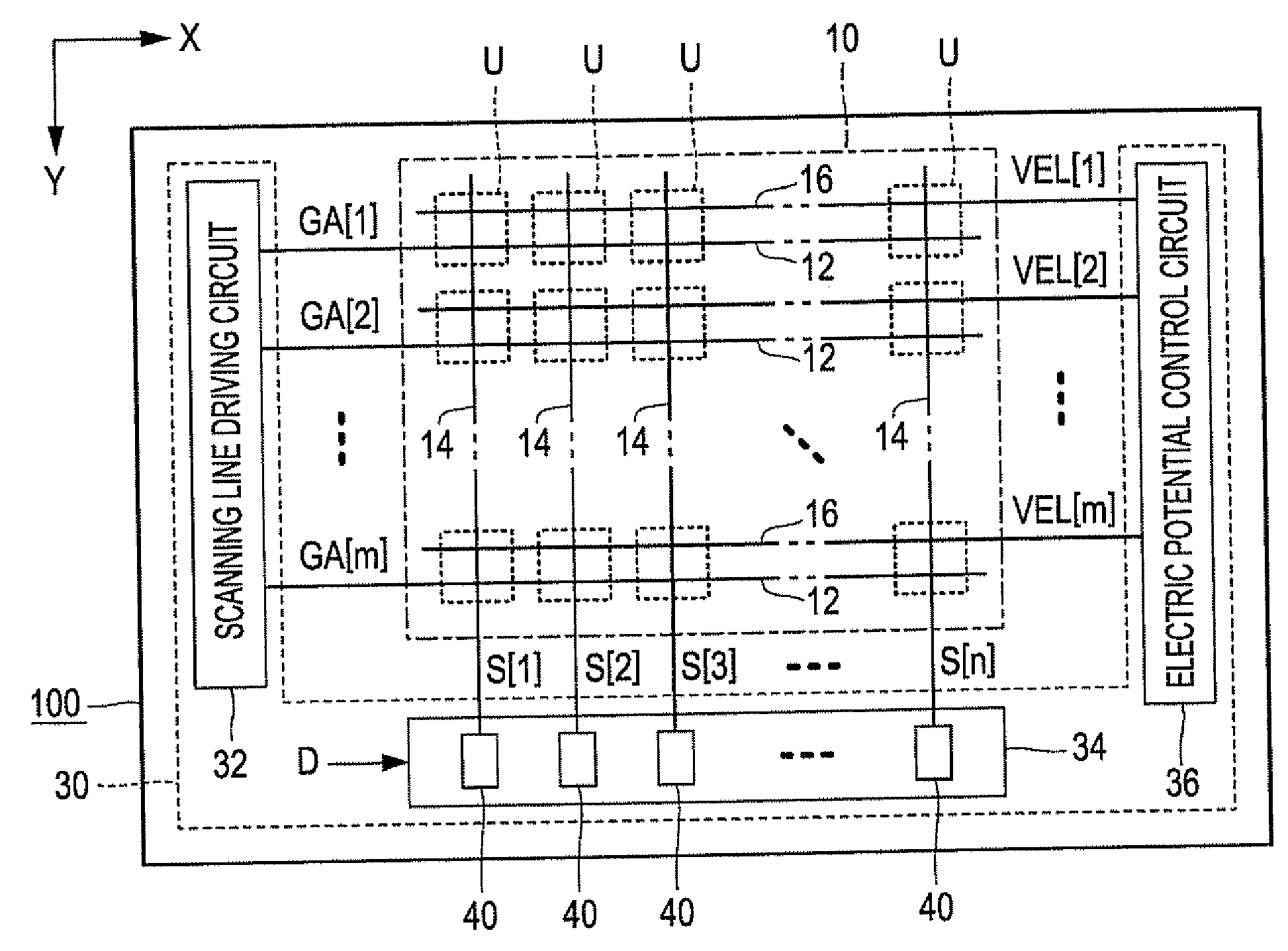
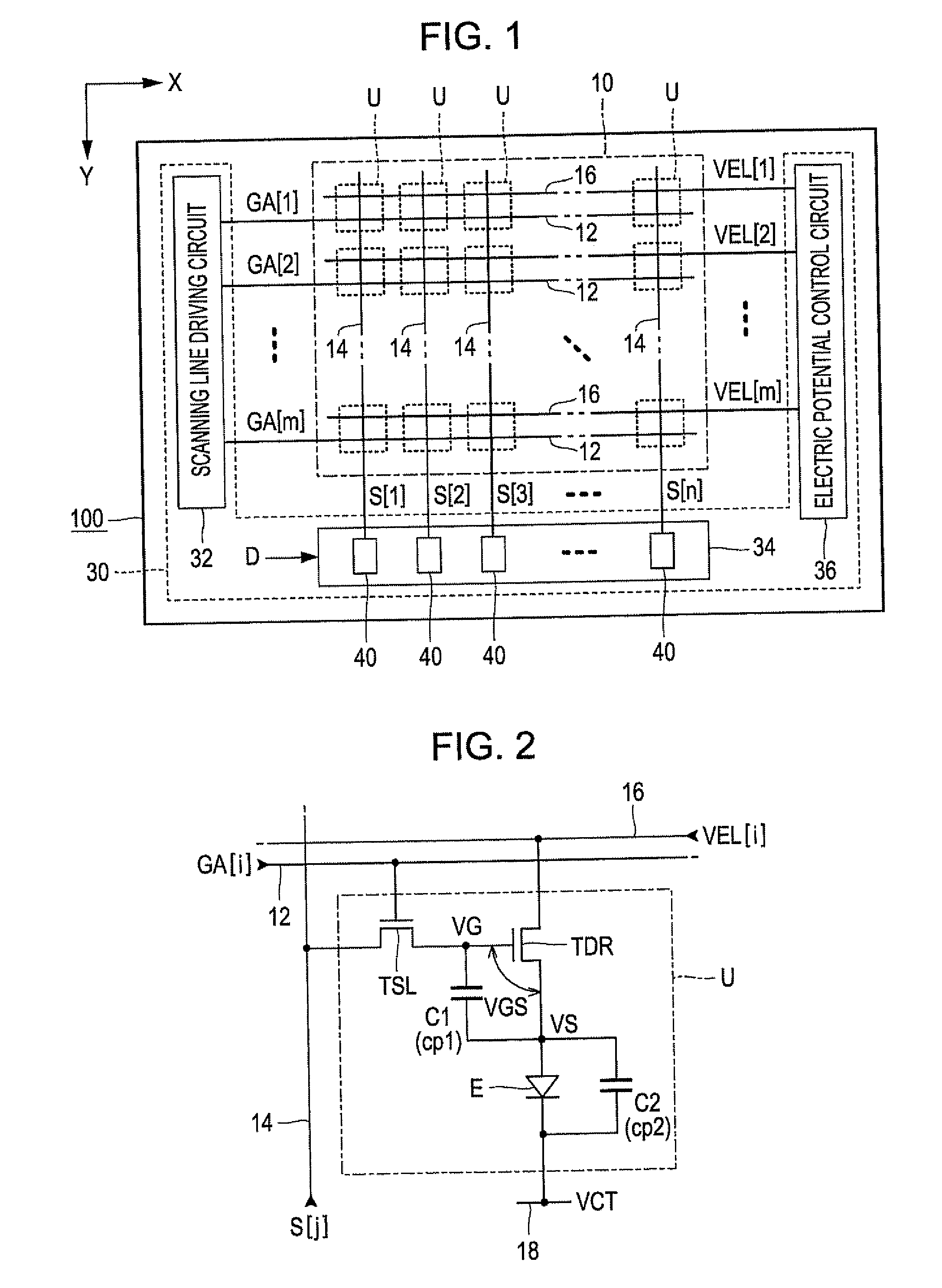
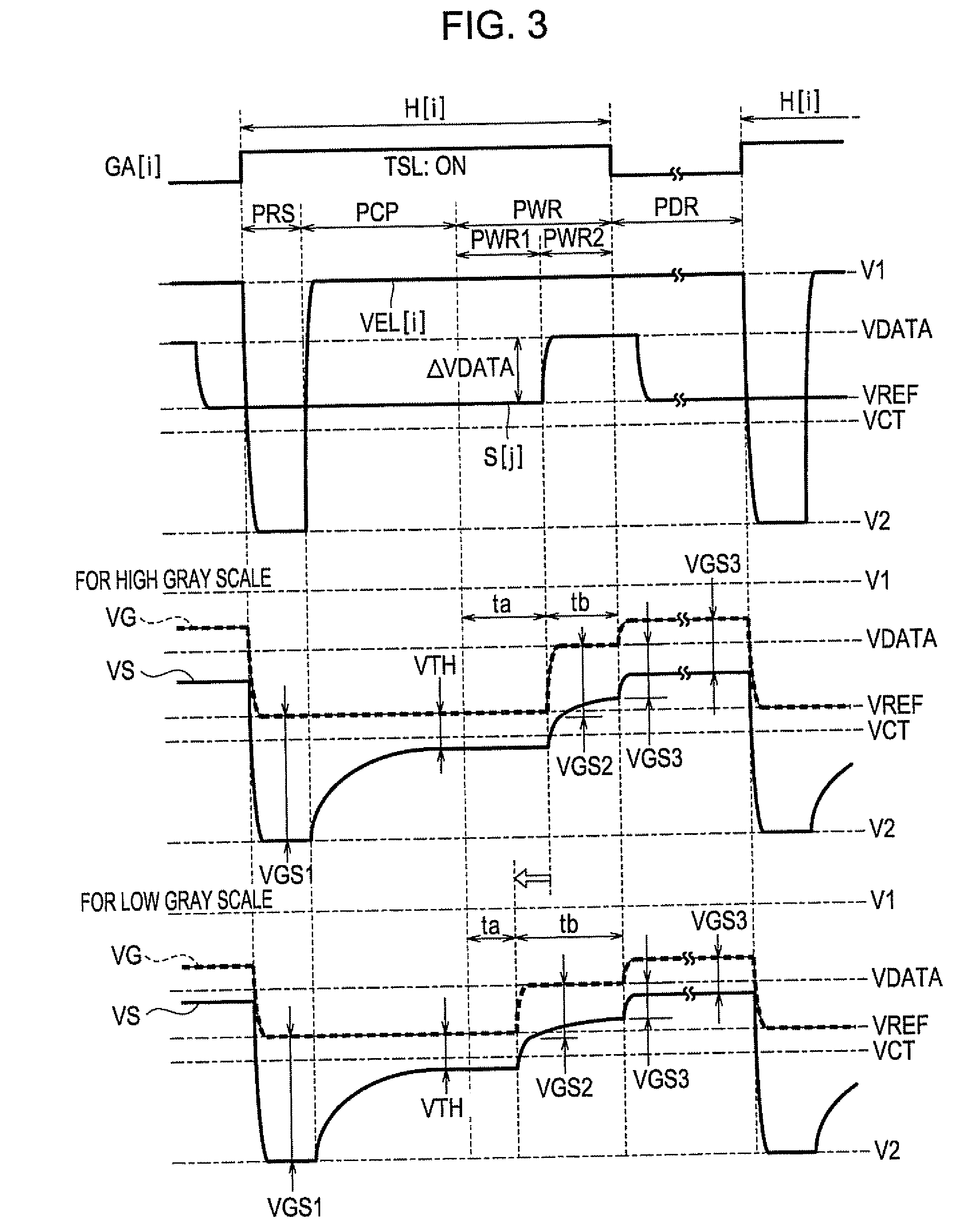
[0099]FIG. 1 is a block diagram showing a light emitting device according to a first embodiment of the invention. The light emitting device 100 is mounted on an electronic apparatus as a display body for displaying an image. As shown in FIG. 1, the light emitting device 100 includes a component unit 10 in which a plurality of pixel circuits U are arranged and a driving circuit 30 that drives the pixel circuits U. The driving circuit 30 includes a scanning line driving circuit 32, a signal line driving circuit 34, and an electric potential control circuit 36. The driving circuit 30 is mounted to be divided into, for example, a plurality of integrated circuits. However, at least one portion of the driving circuit 30 can be configured by thin film transistors formed on a substrate.

[0100]In the component unit 10, m scanning lines 12 extending in a X direction and n signal lines 14 extending in a Y direction perpendicular to the X direction are disposed (here, m and n ...

second embodiment

B: SECOND EMBODIMENT

[0141]Next, a second embodiment of the invention will be described. According to the first embodiment, the first compensation operation is performed for each pixel circuit U in the i-th row in the compensation period PCP within the unit period H[i]. However, when it takes a considerable time for the voltage VGS between the gate and the source of the driving transistor TDR to reach the threshold voltage VTH, the unit period H[i] needs to be set to a long time. In addition, there is a problem that an increase in the precision (an increase of the number of rows) of the pixel circuit U is restricted as the unit period H[i] becomes longer. Thus, according to the second embodiment, by performing the first compensation operation over a plurality of unit periods H, the voltage VGS of the driving transistor TDR is assuredly set to the threshold value VTH while shortening the temporal length of the unit period H.

[0142]FIG. 13 is a circuit diagram of the pixel circuit U acc...

third embodiment

C: THIRD EMBODIMENT

[0154]FIG. 15 is a circuit diagram of a pixel circuit U according to a third embodiment of the invention. As shown in FIG. 15, the pixel circuit U of this embodiment has a configuration in which a control switch TCR2 is added to the pixel circuit U of the first embodiment. The control switch TCR2 is interposed between the gate of the driving transistor TDR and the feed line 54. The control switch TCR2 is an N-channel transistor that controls electrical connection (conduction or non-conduction) between the gate of the driving transistor TDR and the feed line 54. To the feed line 54, the reference electric potential VREF is supplied. In other words, the signal line 14 is also used for the supply of the reference electric potential VREF to the pixel circuit U in the first embodiment or the second embodiment, but the reference electric potential VREP is supplied to each pixel circuit U by using the feed line 54 other than the signal line 14 in this embodiment.

[0155]In...


PUM


Abstract

There is provided a method of driving a pixel circuit that includes a light emitting element; a driving transistor that is connected to the light emitting element in series; a storage capacitor that is interposed between a path, which is formed between the light emitting element and the driving transistor, and a gate of the driving transistor; a selection switch that is interposed between the gate of the driving transistor and a signal line; and a first control switch that is interposed between the gate of the driving transistor and the signal line and is connected to the selection switch in series.

Description

BACKGROUND[0001]1. Technical Field[0002]The present invention relates to a light emitting device such as an organic EL (electroluminescence) device.[0003]2. Related Art[0004]Light emitting devices in which a driving transistor controls the amount of a driving current supplied to a light emitting element suffer from errors (deviations from a target value or non-uniformity between elements) in the electrical characteristics of the driving transistors or the light emitting elements. JP-A-2007-310311 discloses a technique for compensating for errors in the threshold voltage and mobility (furthermore, errors in the amount of driving current) of a driving transistor by setting a voltage across a storage capacitor interposed between the gate and the source of the driving transistor to the threshold voltage of the driving transistor and changing the voltage across the storage capacitor to a voltage corresponding to a gray scale value. However, in JP-A-2007-310311, the errors in the driving ...

Claims


Application Information

Patent Timeline
Patent Type & Authority Applications(United States)
IPC IPC(8): G06F3/038G09G5/10
CPCG09G3/3233G09G2300/0819G09G2300/0852G09G3/30G09G2310/0262G09G2320/043G09G2320/045G09G2300/0866
Inventor ISHIGURO, HIDETOYATABE, SATOSHI
Owner SEIKO EPSON CORP
Why Eureka
Try Eureka