Semiconductor memory device and method of operating the same

a memory device and semiconductor technology, applied in the field of semiconductor memory devices, can solve the problems of “read retention errors, data may be destroyed, read retention errors, etc., and achieve the effect of suppressing read retention errors and reducing access times to second memory

Inactive Publication Date: 2006-06-29
NEC ELECTRONICS CORP
View PDF3 Cites 22 Cited by
  • Summary
  • Abstract
  • Description
  • Claims
  • Application Information

AI Technical Summary

Benefits of technology

[0013] As described above, the sequencer reads out the defect address from the second memory and stores the read defect address in the register before the first address is accessed. When the first memory is accessed, the decoder does not refer to the target address stored in the second memory but refers to the target address stored in the register. Therefore, the number of access times to the second memory is reduced. It is thus possible to suppress the read retention error in the second memory and to hold the defect address well in the second memory, which improves reliability of the semiconductor memory device.
[0016] According to the semiconductor memory device of the present invention, the number of access times to the second memory is reduced. It is thus possible to suppress the read retention error in the second memory holding the defect addresses (replacement addresses).

Problems solved by technology

As a result, the number of access times to the second flash memory 121 is increased, which can cause a “read retention error” as described below.
That is to say, data may be destroyed due to repetitive weak programming during the read operations, which is referred to as the “read retention error”.

Method used


Image

  • Semiconductor memory device and method of operating the same
  • Semiconductor memory device and method of operating the same
  • Semiconductor memory device and method of operating the same

Examples


Embodiment Construction

[0028] The invention will be now described herein with reference to illustrative embodiments. Those skilled in the art will recognize that many alternative embodiments can be accomplished using the teachings of the present invention and that the invention is not limited to the embodiments illustrated for explanatory purposed.

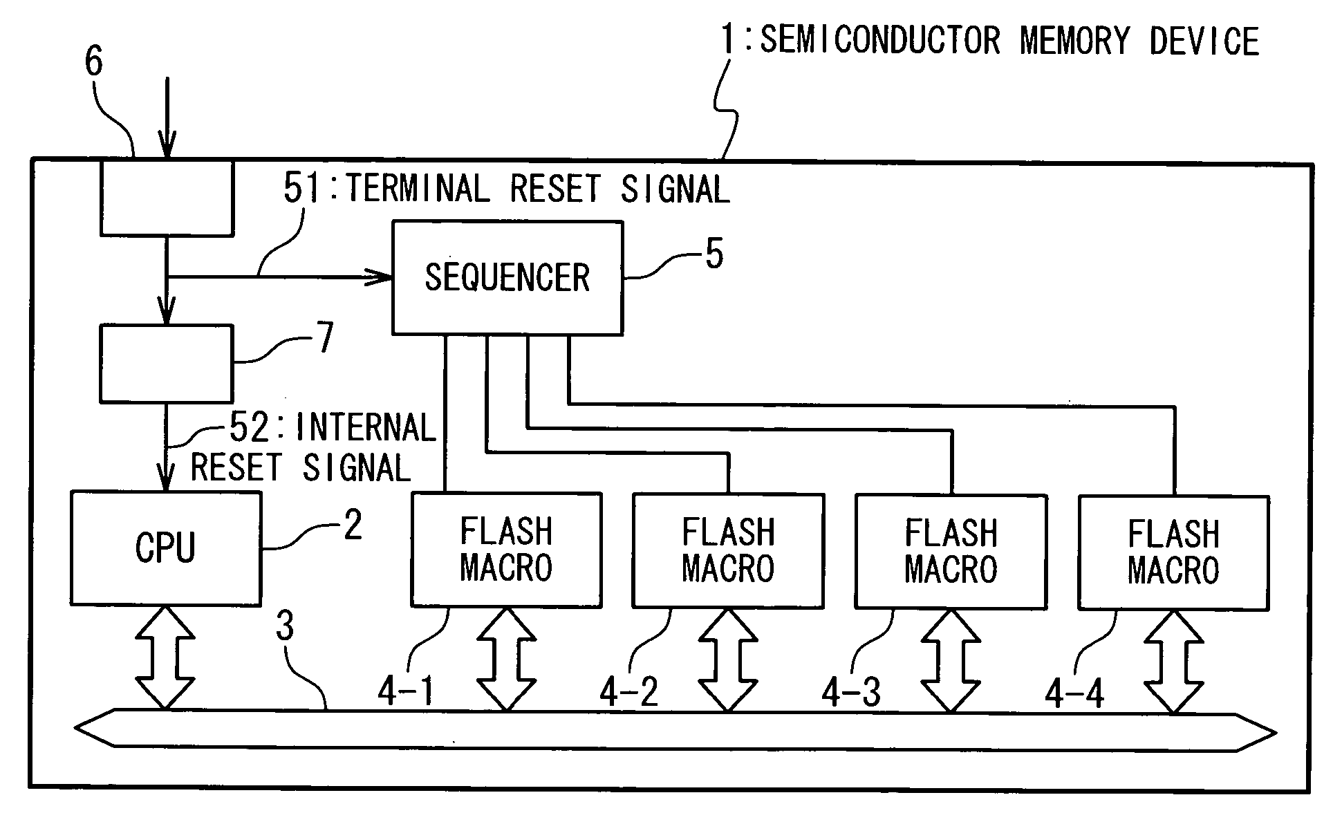
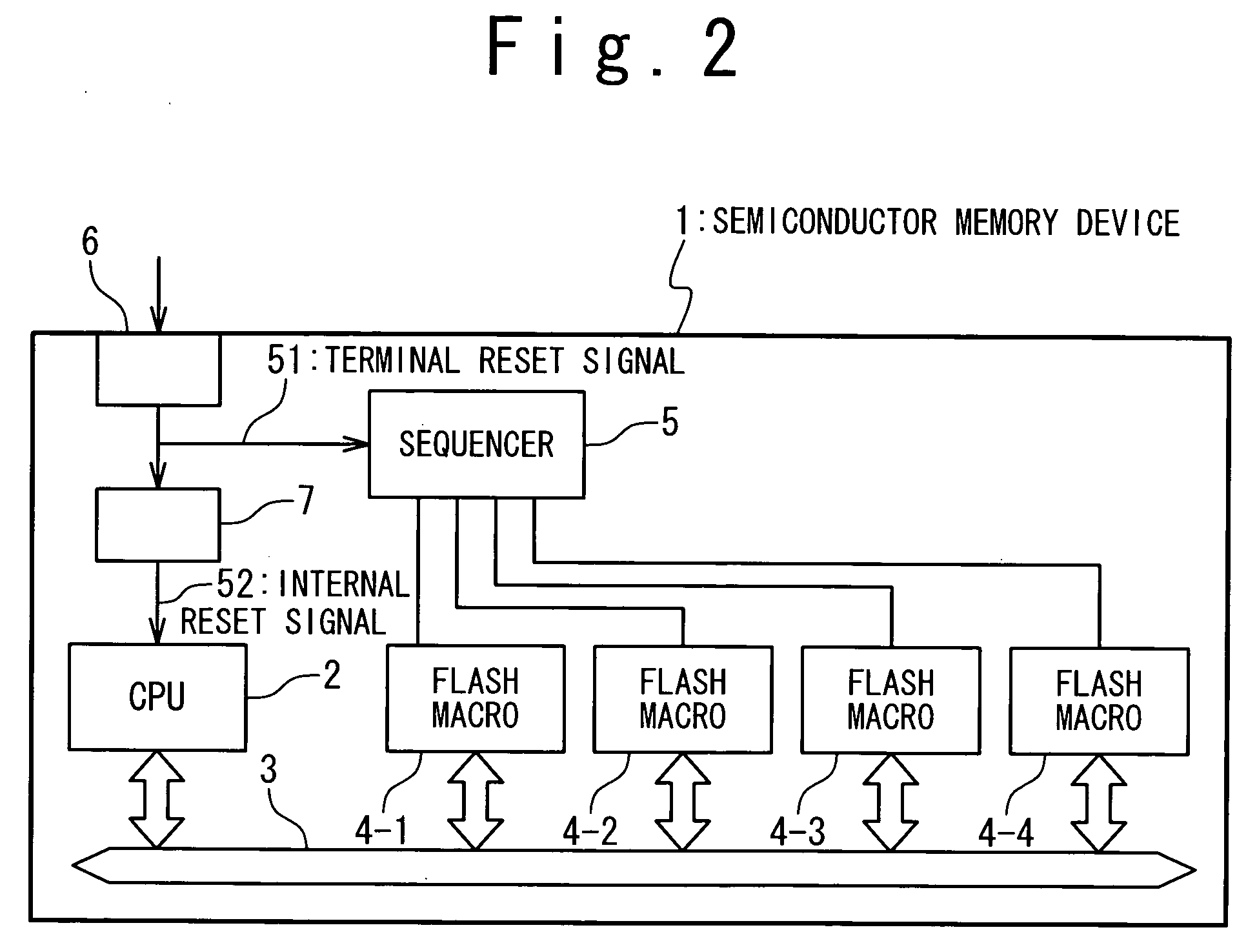
[0029]FIG. 2 is a block diagram showing a configuration of a semiconductor memory device 1 according to the present invention. The semiconductor memory device 1 according to the present invention has a CPU 2, flash macros 4-1 to 4-4, a sequencer 5, a reset controller 6 and an internal reset controller 7. The CPU 2, the flash macros 4-1 to 4-4, the sequencer 5 and the internal reset controller 7 operate in accordance with a clock signal (not shown).

[0030] The reset controller 6 outputs a terminal reset signal 51 as an operation command to the sequencer 5 when a power supply is turned on. The reset controller 6 is exemplified by a switch that is operated by a us...


PUM


Abstract

A semiconductor memory device has: a first memory including a data storage area and a redundant data storage area; a second memory as a nonvolatile memory storing a defect address of the first memory; a register; a sequencer; and a decoder. The sequencer reads out the defect address from the second memory and stores the read defect address in the register. When accessing a target address in the first memory, the decoder compares the target address with the defect address stored in the register, and selects any of the data storage area and the redundant data storage area of the first memory based on a result of the comparison.

Description

BACKGROUND OF THE INVENTION [0001] 1. Field of the Invention [0002] The present invention relates to a semiconductor memory device. In particular, the present invention relates to a semiconductor memory device equipped with a nonvolatile memory, and a method of operating the semiconductor memory device. [0003] 2. Description of the Related Art [0004] A redundancy technique is known in the field of a semiconductor memory device. If there is a problem with a data storage area (memory cell or sector) of a memory, an address of the defective data storage area is replaced with an address of a redundant data storage area (redundant memory cell or redundant sector) in the memory. In order to hold the address of the defective data storage area, a nonvolatile memory such as a flash memory is used which is capable of retaining the memory content even when a power supply is turned off. [0005]FIG. 1 is a block diagram showing a configuration of a semiconductor memory device provided with such a...

Claims


Application Information

Patent Timeline
Patent Type & Authority Applications(United States)
IPC IPC(8): G11C29/00
CPCG11C29/76G11C29/802G11C29/82
Inventor TOMINAGA, KENICHIROU
Owner NEC ELECTRONICS CORP
Why Eureka
Try Eureka