Liquid crystal display device

Active Publication Date: 2010-03-04
JAPAN DISPLAY WEST
View PDF8 Cites 21 Cited by
  • Summary
  • Abstract
  • Description
  • Claims
  • Application Information

AI Technical Summary

Benefits of technology

[0011]In the liquid crystal display device according to the embodiment of the present invention, the common electrode film, the pixel electrode film or both of them are partly removed in the region corresponding to the spacer, and the pixel insulation film is partly

Problems solved by technology

However, for example, in the case of disposing the spacer in the pixel, no concrete consideration is being made with respect to an appropriate position in the pixel for disposing the spacer, a suitable structure for disposing the spacer, and the like.
In some cases, they may break co

Method used


Image

  • Liquid crystal display device
  • Liquid crystal display device
  • Liquid crystal display device

Examples


Example

First Embodiment

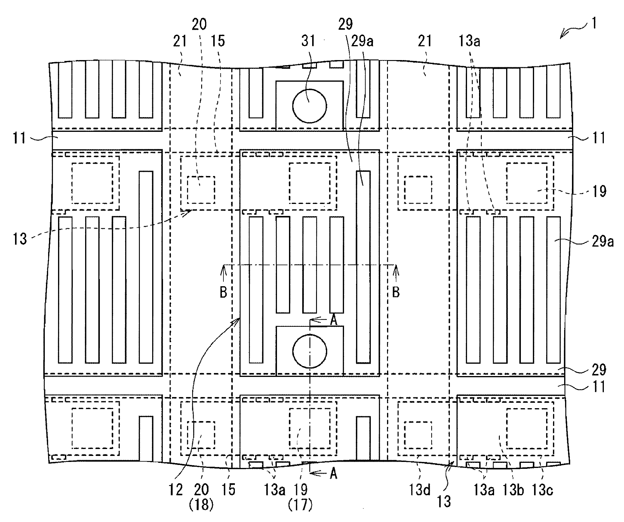
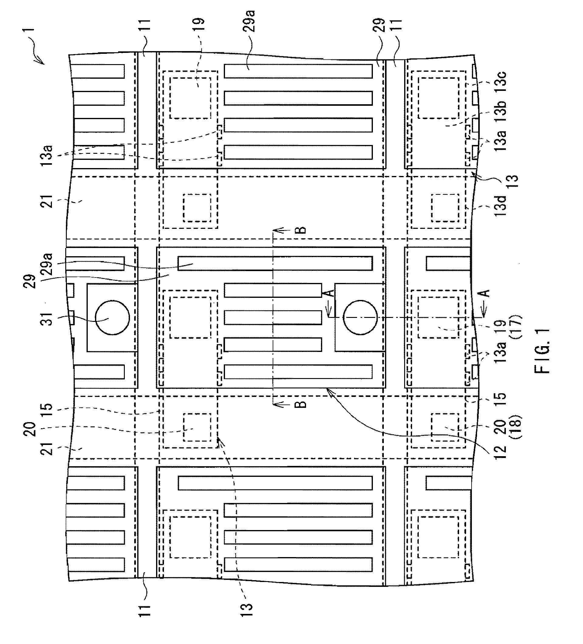
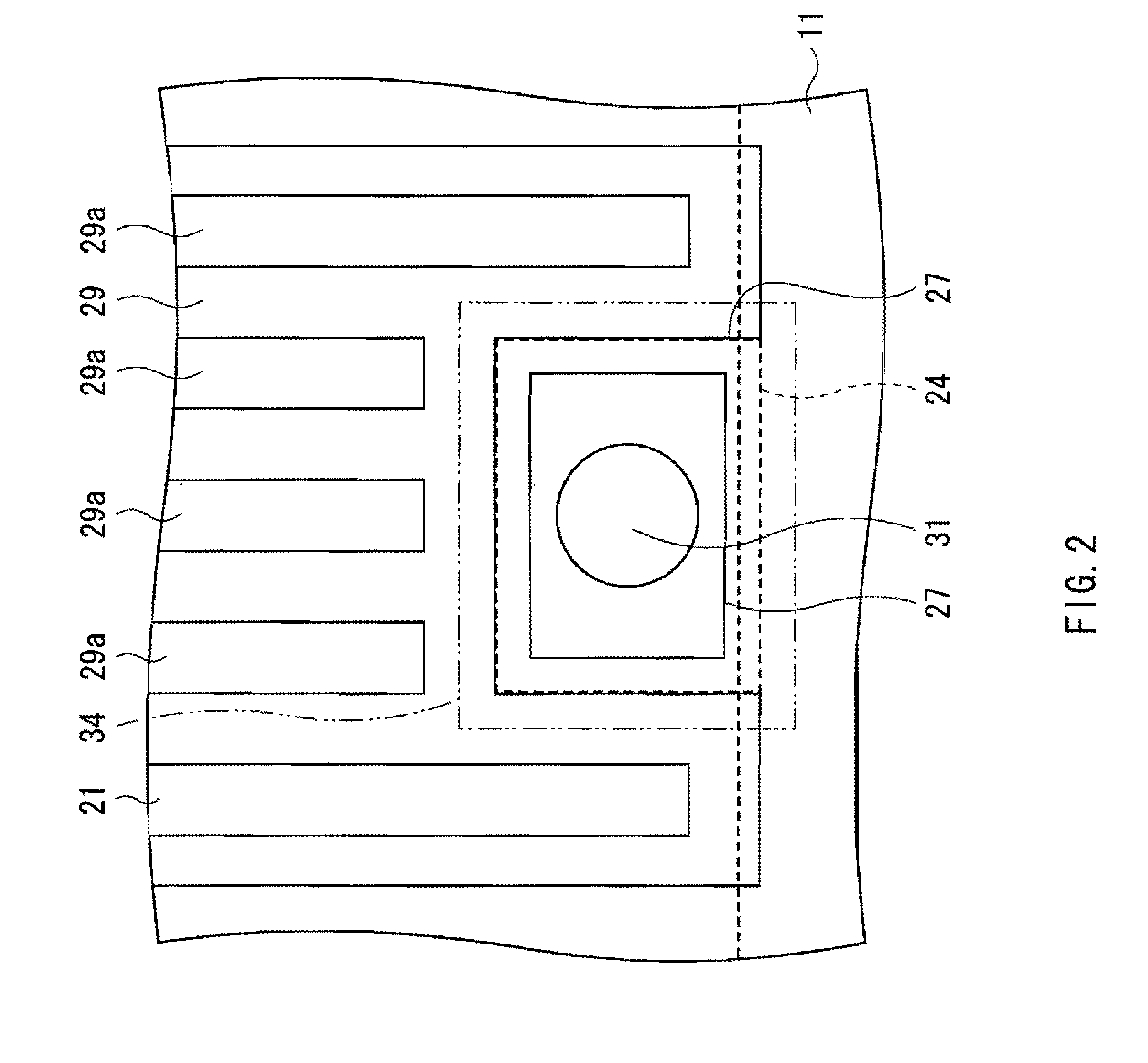
[0026]FIG. 1 is a plan view illustrating a configuration of a main part of a liquid crystal display device 1 according to a first embodiment of the present invention. FIG. 2 is an enlarged view of a spacer part in FIG. 1. FIG. 3 is a cross section taken along line A-A in FIG. 1. FIGS. 1 and 2 illustrate a state where the components above a liquid crystal layer 36 are eliminated.

[0027]As illustrated in FIG. 3, the liquid crystal display device 1 includes a first glass substrate 10 as one concrete example of a “first substrate” of the present invention, and a second glass substrate 35 as one concrete example of a “second substrate” of the present invention. A spacer 31 for maintaining a distance between the first glass substrate 10 and the second glass substrate 35, is disposed between the first glass substrate 10 and the second glass substrate 35. On a side of the first glass substrate 10, a pixel electrode film 29 and a common electrode film 23 formed so as to sandwi...

Example

Second Embodiment

[0063]FIG. 7 illustrates a sectional configuration of a main part in a liquid crystal display device 2 according to a second embodiment. The liquid crystal display device 2 is different from the liquid crystal display device 1 of the first embodiment, with respect to the configuration of a pixel electrode film 40 and a black matrix 41. Specifically, in the liquid crystal display device 2, a pixel electrode film hole is not provided in the pixel electrode film 40. As a result, the pixel electrode film 40 covers all of the part including the top face of the pixel insulation film 26 and an inner wall face and a bottom face of the pixel insulation film hole 27 (the top face of the interlayer insulation film 22 exposed from the pixel insulation film hole 27). In addition, one of end faces of the spacer 31 is in contact with the top face of the pixel electrode film 40 covering the bottom face of the pixel insulation film hole 27. The other configuration is similar to that...

Example

Third Embodiment

[0067]FIG. 9 illustrates a sectional configuration of the spacer 31 portion in a liquid crystal display device 3 according to a third embodiment. The liquid crystal display device 3 is different from the liquid crystal display device 1 of the first embodiment, with respect to a common electrode film 45. Specifically, in the liquid crystal display device 3, the common electrode film hole 24 (FIG. 1) is not provided for the common electrode film 45. As a result, the common electrode film 45 is exposed from the bottom of the pixel insulation film hole 27. In addition, one of the end faces of the spacer 31 is in contact with a top face of the common electrode film 45 exposed at the bottom of the pixel insulation film hole 27. The other configuration is similar to that of the first embodiment (FIG. 3).

[0068]In the third embodiment, the pixel insulation film hole 27 and the pixel electrode film hole 30 are formed, and the pixel insulation film 26 and the pixel electrode fi...


PUM


Abstract

The present invention provides a liquid crystal display device realizing improved reliability by preventing occurrence of a pixel defect. A liquid crystal display includes first and second substrates. A spacer maintains a distance between the first and second glass substrates. A liquid crystal layer is provided between the first and second substrates. A pixel electrode film and a common electrode film are formed over a base insulation film of the first substrate so as to sandwich a pixel insulation film in between. The common electrode film, the pixel electrode film or both of them are partly removed in a region corresponding to the spacer, and the pixel insulation film is partly removed in that region. It prevents the film structure from being broken due to deformation of the base insulation film made of a soft material caused by a pressure applied onto the spacer.

Description

BACKGROUND OF THE INVENTION[0001]1. Field of the Invention[0002]The present invention relates to a liquid crystal display device which performs display by liquid crystal in the transverse electric field mode.[0003]2. Description of the Related Art[0004]One of types of a liquid crystal display device uses liquid crystal in the transverse electric field mode such as an FFS (Fringe Field Switching) mode. FIG. 11 illustrates a partly-enlarged sectional part in a liquid crystal display device 100 in the FFS mode. The liquid crystal display device 100 in the FFS mode is provided with two glass substrates 101a and 101b structuring a liquid crystal display panel. A spacer 102 determining the distance between the glass substrates 101a and 101b is disposed between the glass substrates 101a and 101b. A thin film transistor 103 is formed on a side of the glass substrate 101a. On the thin film transistor 103, an interlayer insulation film 104 for flattening the roughness is formed by an organic ...

Claims


Application Information

Patent Timeline
IPC IPC(8): G02F1/1343
CPCG02F1/13338G02F1/13394G02F2001/13312G02F2201/503G02F2001/134372G02F2201/50G02F2001/13398G02F1/13312G02F1/13398G02F1/134372
Inventor KANAYA, YASUHIROYAGI, KEIICHI
Owner JAPAN DISPLAY WEST
Why Eureka
Try Eureka